Method of manufacturing flash memory device
A memory device and flash technology, applied in semiconductor/solid-state device manufacturing, electrical components, mattresses, etc., can solve problems such as difficulty in ensuring alignment margins
Inactive Publication Date: 2007-09-05
SK HYNIX INC
View PDF2 Cites 4 Cited by
- Summary
- Abstract
- Description
- Claims
- Application Information
AI Technical Summary
Problems solved by technology
This makes it difficult to secure an alignment margin between the drain contact plug and the bit line
Method used
View moreImage
Smart ImageViewing Examples


Examples
no. 1 example
Login to View More PUM
 Abstract
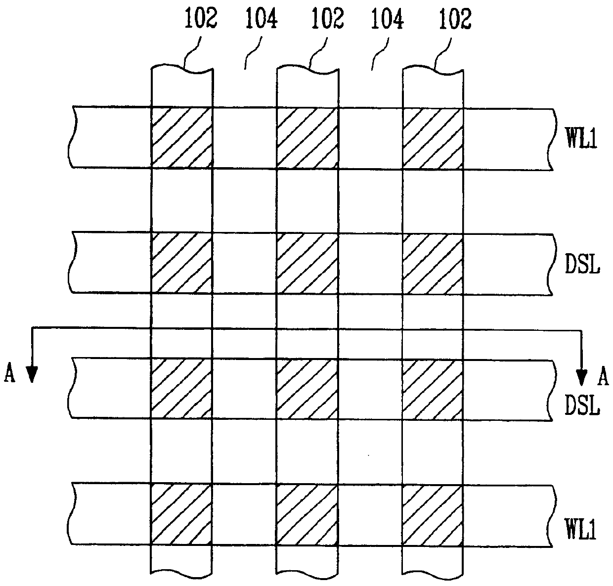
A method of manufacturing a flash memory device includes etching an insulating layer provided over a substrate to form a contact hole to define a contact hole exposing a junction region formed on the substrate. The contact hole is filled with a first conductive material, the first conductive material contacting the junction region and extending above an upper surface of the contact hole. The first conductive material is etched to partly fill the contact hole, so that the first conductive material fills a lower portion of the contact hole, wherein an upper portion of the contact hole remains not filled due to the etching of the first conductive material, wherein the etched first conductive material defines a contact plug. A first dielectric layer and a second dielectric layer are formed over the contact plug, thereby filling the upper portion of the contact hole. Part of the first and second dielectric layers is etched to expose the contact plug and the upper portion of the contact hole. A second conductive material is formed on the contact plug and filling the upper portion of the contact hole to form a bit line.
Description
technical field The present invention relates to a method of manufacturing a flash memory device. Background technique Flash memory devices have become highly integrated and multifunctional. Therefore, the reduced size of the contact holes makes it difficult to fill the contact holes. It also becomes difficult to reduce the resistance of the drain contact plug. This makes it difficult to secure an alignment margin between the drain contact plug and the bit line. Contents of the invention An embodiment of the present invention relates to a method of fabricating a flash memory device that can obtain a drain contact by using a method of partially removing only the top surface of the contact via a maskless selective etch process followed by a self-aligned etch process. Alignment margin between plug and bit line to reduce defects caused by misalignment. Another embodiment of the present invention relates to a method of manufacturing a flash memory device, which can reduc...
Claims
Login to View More Application Information
Patent Timeline
 Patent Type & Authority Applications(China)
IPC IPC(8): H01L21/8247H01L21/768
CPCA47C21/048A47C27/00B32B7/00
Inventor 朴仙美全裕男金南经金世埈
Owner SK HYNIX INC
Features
- R&D
- Intellectual Property
- Life Sciences
- Materials
- Tech Scout
- Unparalleled Data Quality
- Higher Quality Content
- 60% Fewer Hallucinations
Learn More Browse by: Latest US Patents, China's latest patents, Technical Efficacy Thesaurus, Application Domain, Technology Topic, Popular Technical Reports.
© 2025 PatSnap. All rights reserved.Legal|Privacy policy|Modern Slavery Act Transparency Statement|Sitemap|About US| Contact US: help@patsnap.com