Supercharge Your Innovation With Domain-Expert AI Agents!

Strip format of package board and array of the same

A technology of packaging boards and arrays, applied in the direction of identifying devices, instruments, electrical components, etc., can solve problems such as increasing strip structures that have not been tried

Inactive Publication Date: 2007-10-17
SAMSUNG ELECTRO MECHANICS CO LTD
View PDF1 Cites 6 Cited by
  • Summary
  • Abstract
  • Description
  • Claims
  • Application Information

AI Technical Summary

Problems solved by technology

[0009] Therefore, in the conventional process of assembling the semiconductor package board, since the standard size of the semiconductor package board strip structure and the panel remains constant, no attempt has been made to increase the number of semiconductor package board strip structures mountable on the panel.

Method used


Image

  • Strip format of package board and array of the same
  • Strip format of package board and array of the same
  • Strip format of package board and array of the same

Examples


Embodiment Construction

[0025] Hereinafter, the present invention will be described in detail with reference to the accompanying drawings.

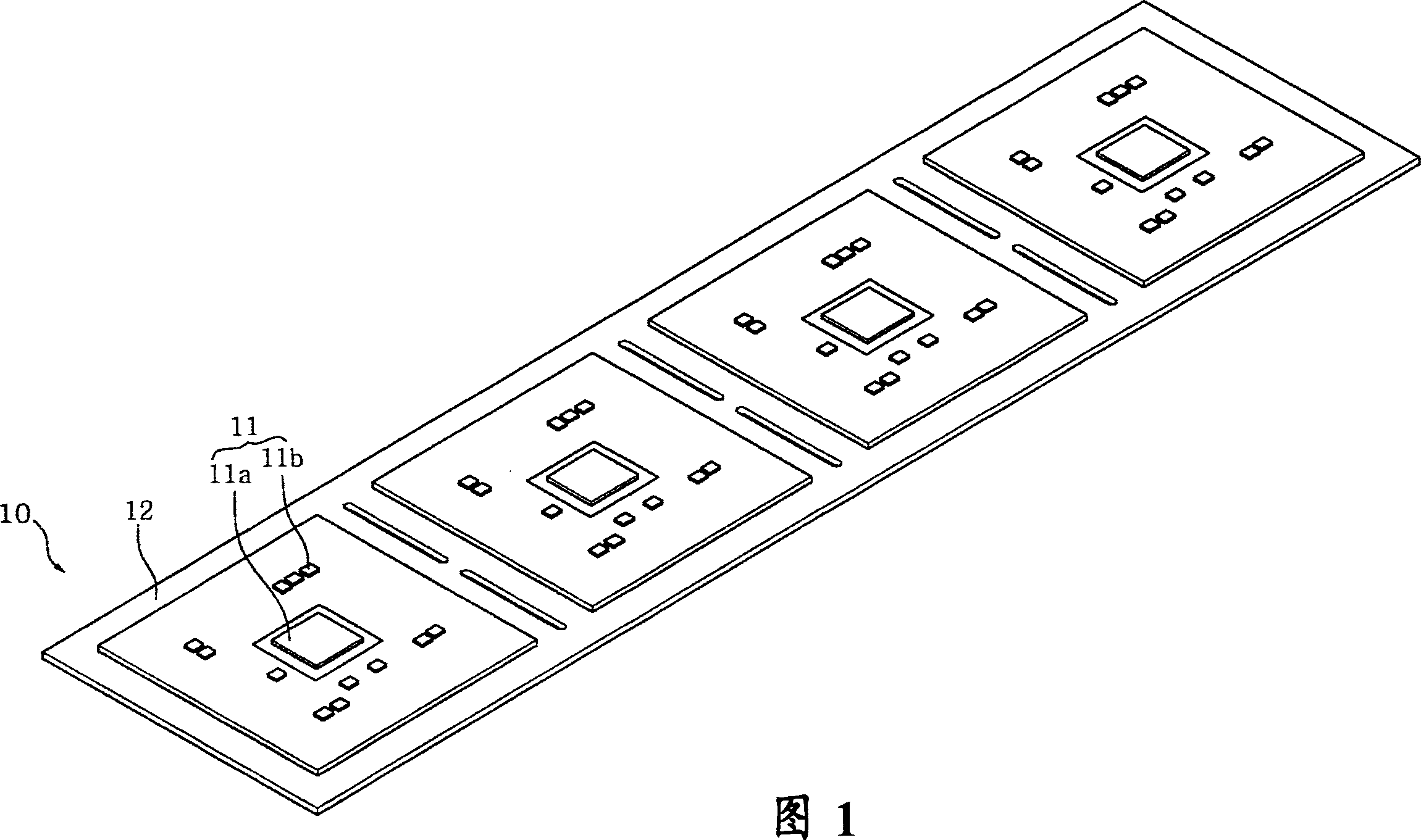
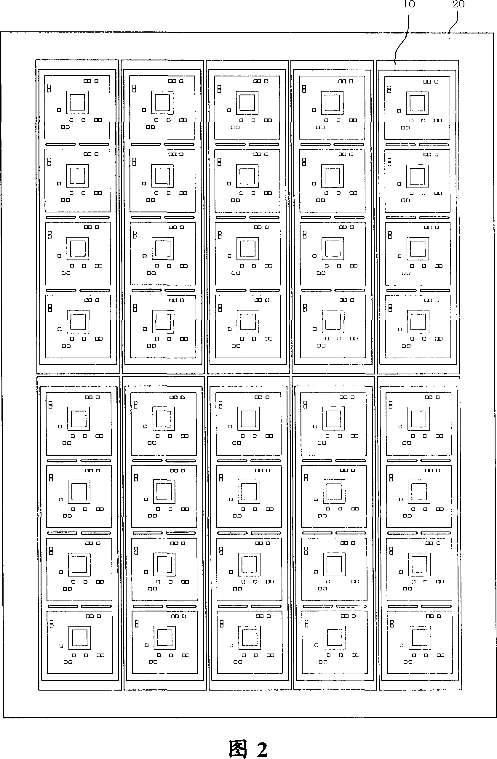
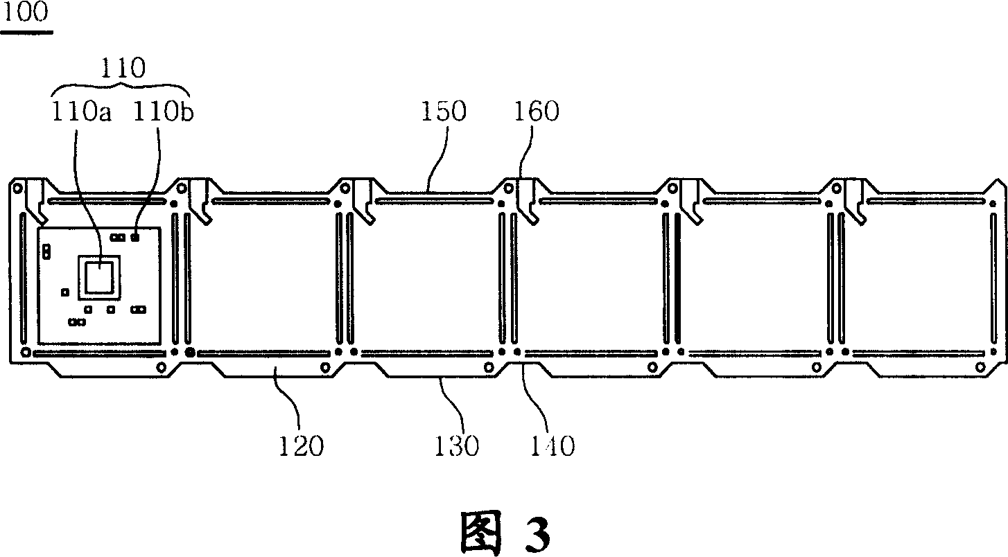
[0026] For reference only, FIG. 3 shows a strip structure of a PBGA (Plastic Ball Grid Array) semiconductor package board according to a first embodiment of the present invention. Figure 4 shows an interconnected strip structure. FIG. 5 shows a strip structure of PBGA semiconductor package boards arranged on a panel. 6 to 8 show usage examples of a CSP (Chip Scale Package) semiconductor package board according to a second embodiment of the present invention.

[0027] As described above, the present invention provides a method of increasing the number of strip structures of semiconductor package boards to be arrayed on a panel. In detail, the present invention is characterized in that the bar structure is formed into a predetermined shape so that an unnecessary part can be removed to the maximum from a vacant area provided in an area surrounding the bar structu...


PUM


Abstract

Disclosed herein is a strip format of a semiconductor package board and an array thereof, in which a dummy area of the strip format of the semiconductor package board is formed into a predetermined shape such that, when several strip formats of semiconductor package boards are arranged on a panel, the number of strip formats of semiconductor package boards arranged on the panel can be increased.

Description

[0001] Related Application Cross Reference [0002] This application claims the benefit of Korean Patent Application No. 10-2006-0033266, filed Apr. 12, 2006, entitled "A PACKAGE STRIP FORMAT AND ITS ARRAY," the entire contents of which are incorporated herein Reference. technical field [0003] The present invention generally relates to a strip format of a semiconductor package board (strip format) and an array thereof, and more particularly, to a strip format of a semiconductor package board and an array thereof, wherein the dummy of the strip format of the semiconductor package board ) region is formed in a predetermined shape so that when several strip structures of the semiconductor package board are arranged on the panel, the number of strip structures of the semiconductor package board arranged on the panel can be increased. Background technique [0004] As is well known to those skilled in the art, the conventional strip structure of a semiconductor package board ha...

Claims


Application Information

Patent Timeline
IPC IPC(8): H01L23/498H01L23/492H01L25/00G09F9/00
CPCH01L23/49838H01L2924/0002H01L23/13H01L2924/00H01L21/76H01L21/77
Inventor 姜太赫廉光燮沈揆铉崔凤圭黄奎一金元熙
Owner SAMSUNG ELECTRO MECHANICS CO LTD
Features
  • R&D
  • Intellectual Property
  • Life Sciences
  • Materials
  • Tech Scout
  • Unparalleled Data Quality
  • Higher Quality Content
  • 60% Fewer Hallucinations
Learn More