A differential signal interface circuit

A differential signal and interface circuit technology, applied in the direction of logic circuit connection/interface layout, logic circuit coupling/interface using field effect transistors, etc., can solve the problems of no level conversion, circuit complexity, cost increase, etc., to achieve reduction The effects of small working voltage, simplified circuit structure and high working speed

Active Publication Date: 2007-10-24
SANECHIPS TECH CO LTD
View PDF2 Cites 12 Cited by
  • Summary
  • Abstract
  • Description
  • Claims
  • Application Information

AI Technical Summary

Problems solved by technology

[0005] 1. Two modules are used to process different types of input signals separately, which complicates the circuit;
[0006] 2. There is no built-in level conversion circuit from high power supply voltage signal to low power supply voltage signal, which makes the scope of application of the patent smaller, which is no longer suitable for the development of the current technology to sub-micron technology;
[0007] 3. It is realized by BiCMOS process, which increases the cost and cannot be used in modern CMOS process
It is known from the patent description that the patent can only receive LVDS signals and has no level conversion function

Method used


Image

  • A differential signal interface circuit
  • A differential signal interface circuit
  • A differential signal interface circuit

Examples


Embodiment Construction

[0033] In order to further illustrate the technical means and effects adopted by the present invention to achieve the intended invention purpose, the present invention will be described in detail below in conjunction with the accompanying drawings and preferred embodiments.

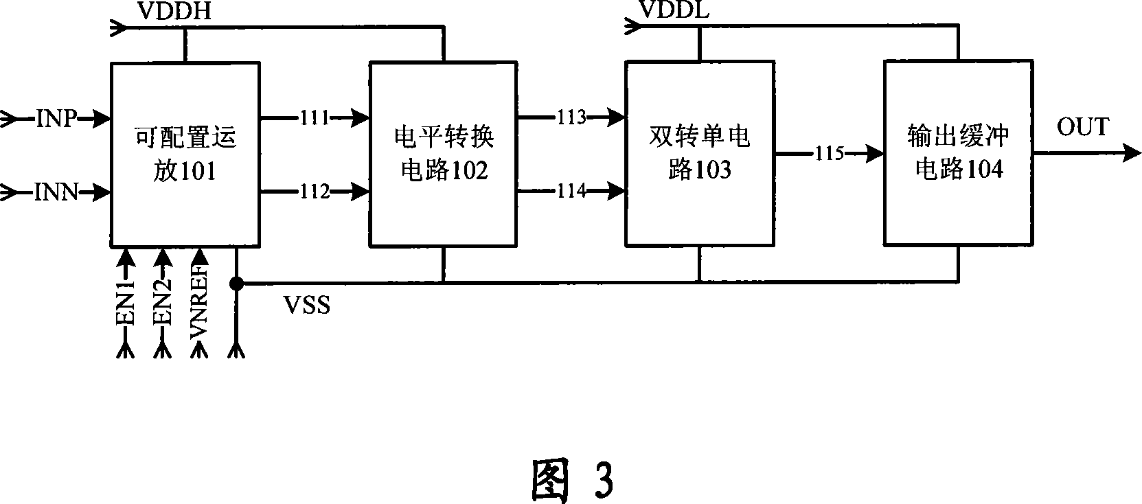
[0034] In order to achieve the purpose of the above invention, the present invention proposes a new type of interface circuit, which mainly includes a configurable operational amplifier 101, a level conversion circuit 102, a double-to-single circuit 103 and an output buffer circuit 104. The specific circuit is shown in FIG. 3 .

[0035]The specific connection of the interface circuit is as follows: the external high-level differential signals INP and INN are input to the configurable operational amplifier 101, and the external control signals EN1, EN2 and the reference voltage VNREF are input to the configurable operational amplifier 101; the configurable operational amplifier 101 outputs a set of differen...


PUM


Abstract

The disclosed differential signal interface circuit comprises mainly: a configurable operational amplifier (OA) with input from INP, INN, EN1, EN2, VDDH and VNREF, to output differential signal to next circuit; a level switch circuit with VDDH as input to output differential signal to next circuit, and a double-to-one circuit to output single-port signal. This invention is compatible to LVDS and LVPECL signal to converse into CMOS logic signal, and can be used in high-speed data transmission.

Description

technical field [0001] The invention relates to a differential signal interface circuit applied to high-speed data transmission between chips in a communication circuit, which can be compatible with different types of input signals such as LVDS and LVPECL and convert them into CMOS logic signals by configuring different working modes. Background technique [0002] With the development of communication technology, the data transmission speed between chips is getting faster and faster, and now the use of differential signals is becoming more and more extensive. One of the advantages of differential signaling is that it has a smaller amplitude, which maximizes data transmission speed. In addition, the differential signal has anti-interference and anti-noise performance. In the field of communication, the most widely used differential signals are LVDS and LVPECL signals. Among them, LVDS refers to low-voltage differential signal, low-voltage differential signal; LVPECL refers ...

Claims


Application Information

Patent Timeline
Patent Type & Authority Applications(China)
IPC IPC(8): H03K19/0175H03K19/0185
Inventor 周海牛陈志荣
Owner SANECHIPS TECH CO LTD
Why Eureka
Try Eureka