Improved ion beam utilization during scanned ion implantation

A technology of ion implantation and ion beam, which is applied in the direction of discharge tubes, electrical components, circuits, etc., can solve the problems of easy understanding, reduction of processing amount, waste of resources, etc.

Active Publication Date: 2007-10-24
AXCELIS TECHNOLOGIES
View PDF0 Cites 7 Cited by
  • Summary
  • Abstract
  • Description
  • Claims
  • Application Information

AI Technical Summary

Problems solved by technology

However, since the workpiece is generally circular (except, for example, where the alignment notch is located), it is understood that the ion beam "overshoots" or misses the impact on the workpiece, i.e., the substrate (e.g., the substrate) most of the time. , when the ion beam does not scan the widest part of the workpiece)
This reduces processing throughput and wastes resources

Method used


Image

  • Improved ion beam utilization during scanned ion implantation
  • Improved ion beam utilization during scanned ion implantation
  • Improved ion beam utilization during scanned ion implantation

Examples


Embodiment Construction

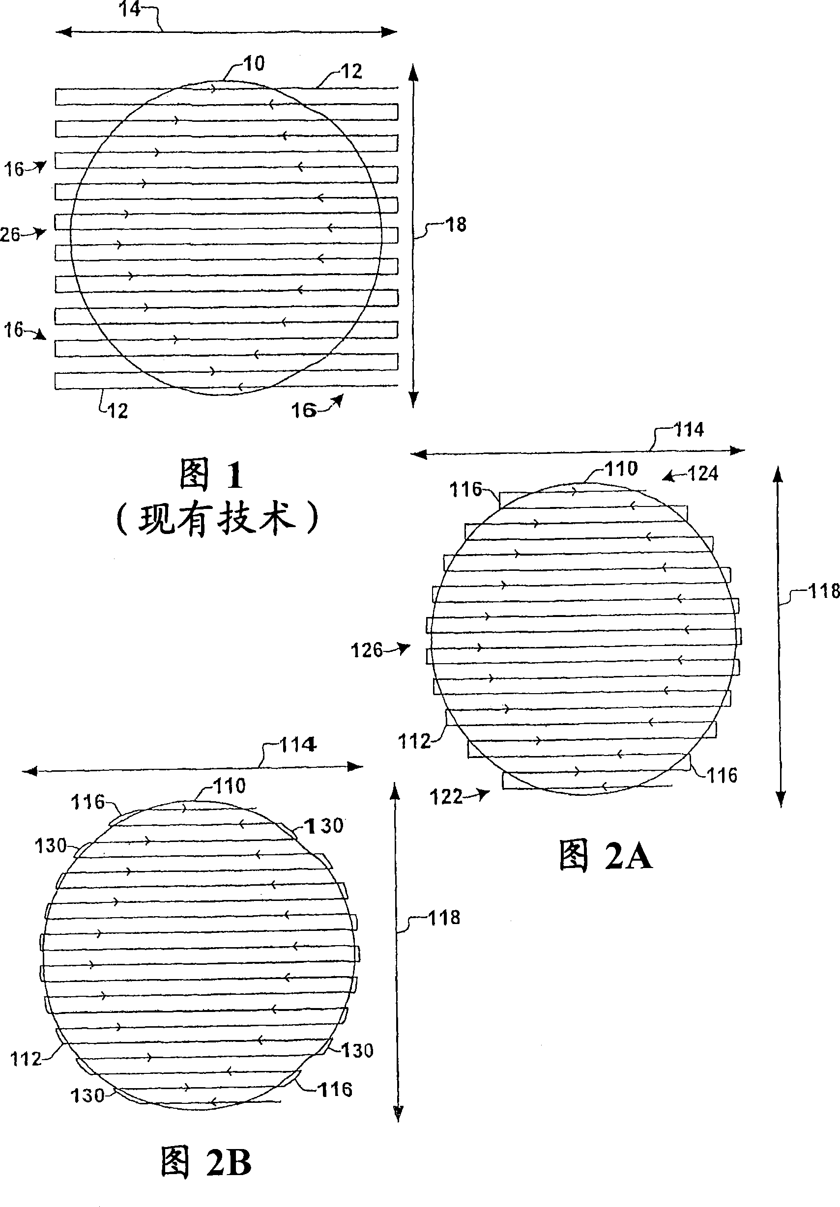
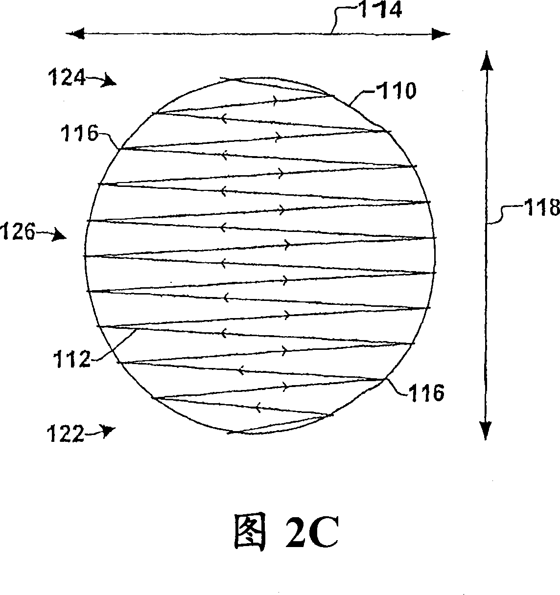
[0020] The present invention involves moving a workpiece, ie, a substrate, relative to a substantially stationary ion beam such that the resulting scan pattern resembles the shape of the workpiece. One or more aspects of the invention will now be described with reference to the drawings, wherein like reference numerals refer to like elements throughout. Note that the drawings and the following description are illustrative only and should not be considered limiting. In the following description, for purposes of explanation, numerous specific details are set forth in order to provide a thorough understanding of the invention. However, it will be understood by those skilled in the art that the present invention may be practiced without these specific details. Accordingly, it should be understood that there are many variations to the systems and methods of the invention in addition to those described herein, and such variations are within the scope of the invention and the append...


PUM


Abstract

The present invention is directed to implanting ions in a workpiece in a serial implantation process in a manner that produces a scan pattern that resembles the size, shape and / or other dimensional aspects of the workpiece. This improves efficiency and yield as an ion beam that the workpiece is oscillated through does not significantly''overshoot'' the workpiece. The scan pattern may be slightly larger than the workpiece, however, so that inertial effects associated with changes in direction, velocity and / or acceleration of the workpiece as the workpiece reverses direction in oscillating back and forth are accounted for within a small amount of''overshoot''. This facilitates moving the workpiece through the ion beam at a relatively constant velocity which in turn facilitates substantially more uniform ion implantation.

Description

technical field [0001] The present invention relates generally to semiconductor processing systems, and more particularly to control of movement of a substrate relative to an ion beam during ion implantation. Background technique [0002] In the semiconductor industry, various fabrication processes are typically performed on a substrate (eg, a semiconductor workpiece) in order to achieve various effects on the substrate. For example, processing (such as implantation) can be performed on or within the substrate to obtain specific features, such as by implanting specific types of ions to limit the diffusion capacity of the dielectric layer on the substrate. Typically, the ion implantation process is performed either in a batch process in which a plurality of substrates are processed simultaneously, or in a continuous process in which a single substrate is processed. For example, conventional high-energy or high-current batch ion implanters can be used to obtain short ion beam...

Claims


Application Information

Patent Timeline
Patent Type & Authority Applications(China)
IPC IPC(8): H01J37/317H01J37/302
CPCH01J37/3171H01J37/302H01J2237/20228H01J2237/30488H01L21/265
Inventor M·葛瑞夫A·芮
Owner AXCELIS TECHNOLOGIES
Why Eureka
Try Eureka