

Multi-layer flexible circuit board and its producing method
A flexible circuit board and outer layer technology, which is applied in the direction of multilayer circuit manufacturing, printed circuit, electrical components, etc., can solve the problems of affecting the product yield rate, circuit etching circuit break, and dry film pressing, so as to improve reliability , Simple operation, good reinforcement effect
Active Publication Date: 2007-10-31
NAIR ENERGY EQUIP
View PDF0 Cites 9 Cited by
- Summary
- Abstract
- Description
- Claims
- Application Information
AI Technical Summary
Problems solved by technology
[0004] The gold finger area of the multi-layer flexible circuit board is a dynamic area. Generally, during the design and manufacturing process, the inner layer corresponding to the gold finger area is washed away to avoid it, so as to meet the thickness requirements and bending performance requirements of the gold finger are
Method used
View moreImage
Smart ImageViewing Examples

Examples
 PUM
| Property | Measurement | Unit |
|---|---|---|
| Thickness | aaaaa | aaaaa |
| Thickness | aaaaa | aaaaa |
| Thickness | aaaaa | aaaaa |
Abstract
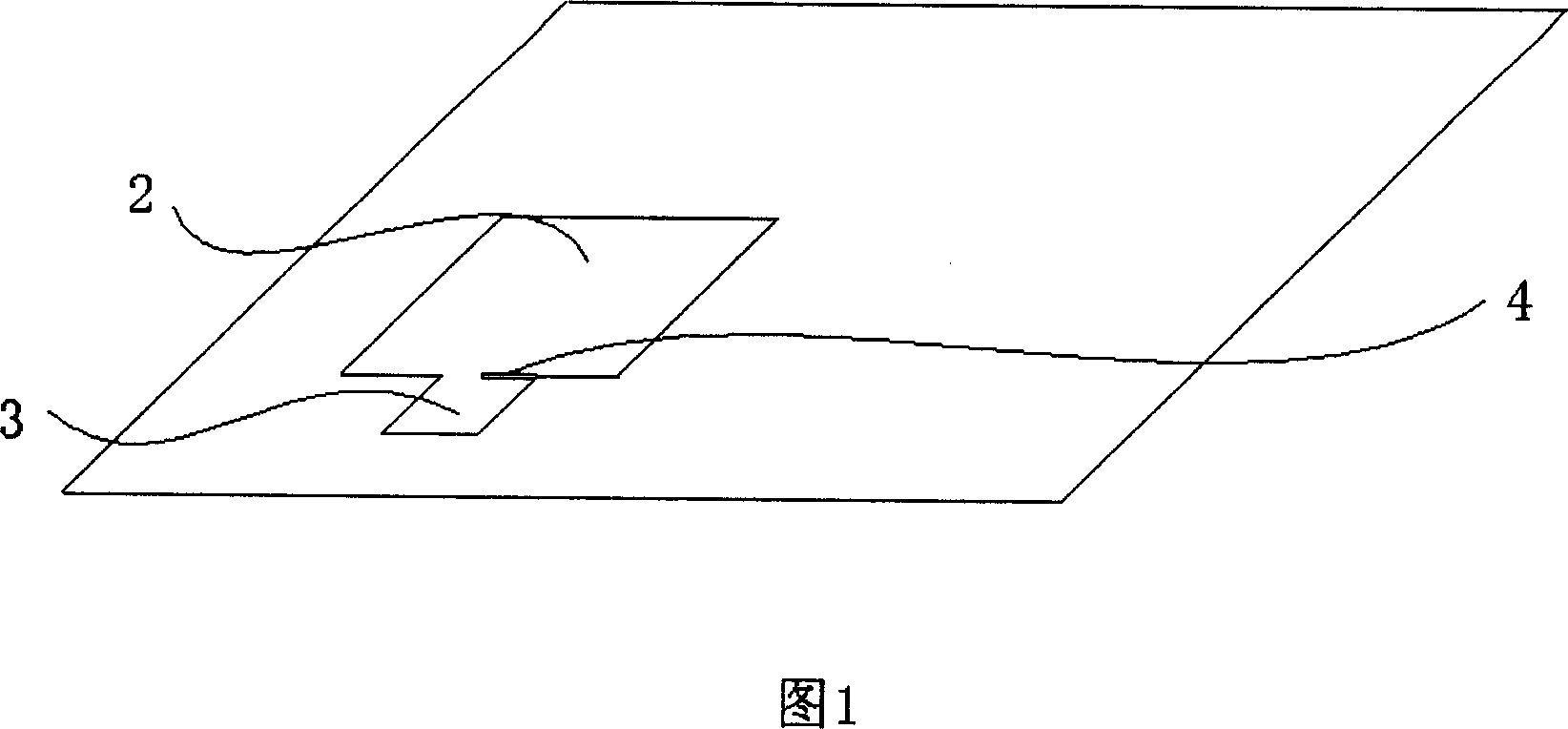
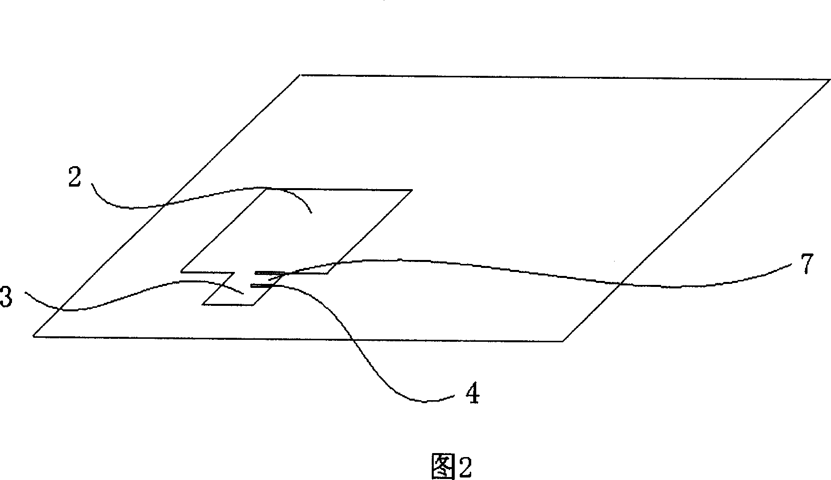
The invention discloses a multiple layer flexible circuitry board and preparing method, it includes three layers or more than three layers of single flexible circuitry board, and each of which is adhibited with half solid piece, the first outer layer possesses golden finger area for setting golden finger, the inner layer separately includes entity and die-cutting piece which can be tore with each other; the second layer includes entity and die-cutting piece which can be tore with each other, the die-cutting piece of inner layer and the second layer aligns at the golden finger area of the first outer layer. During the pressure of the multiple layer flexible circuitry board, the inner layer and the second layer which aligns at the golden finger area of the first outer layer are always kept, that is the die-cutting piece, so the altitude difference between the golden finger area and other area can be decreased, so dry film is pressed on outer layer, the perfect fill will be realized, and without air bubble, later perfect line etching is guaranteed, the problem of ill plough of line can be avoided.
Description
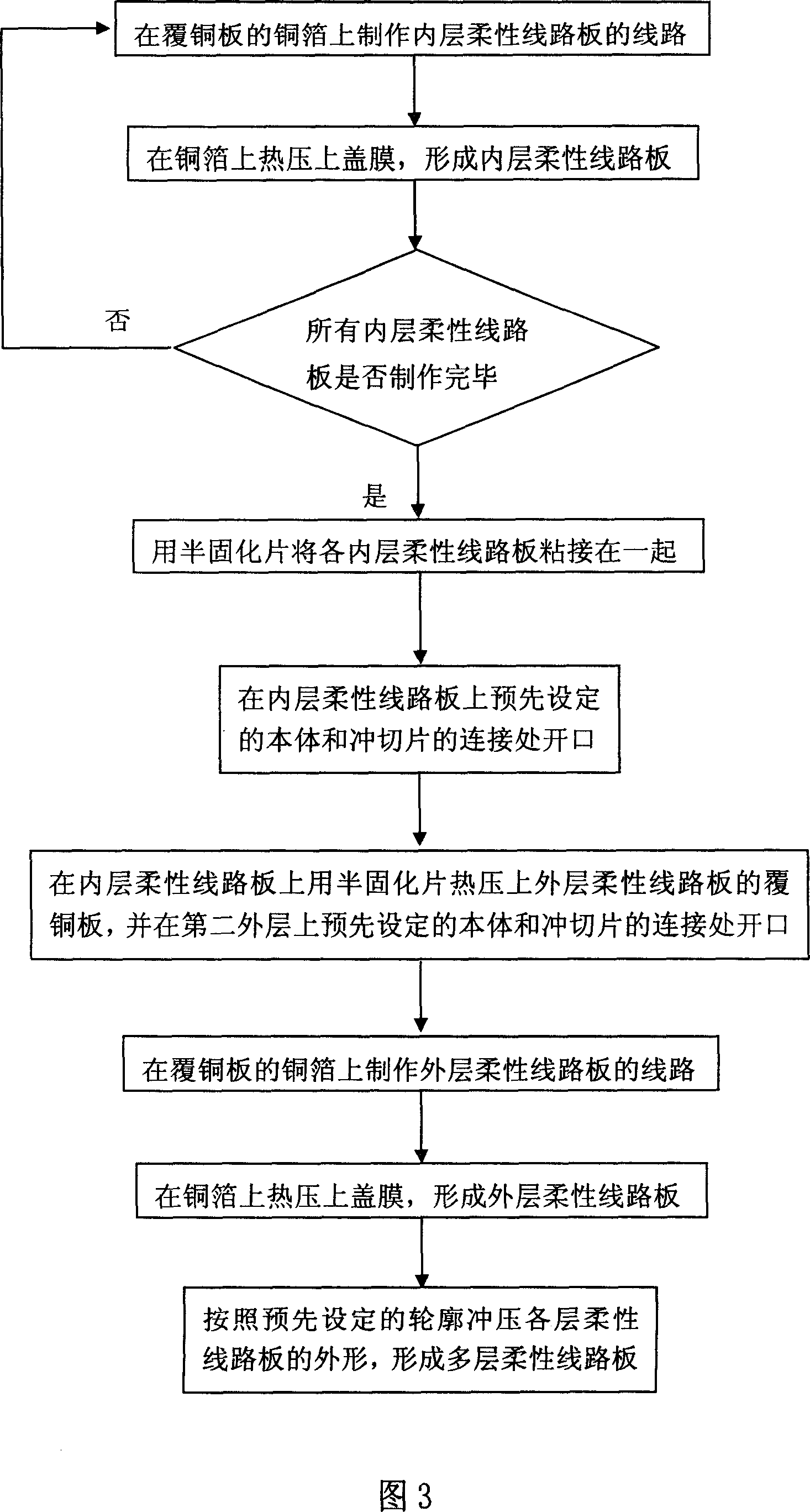
technical field [0001] The invention relates to a multilayer flexible circuit board and a manufacturing method thereof. Background technique [0002] With the miniaturization and lightweight development of various electronic devices, flexible circuit boards with small size, high heat resistance, superior bending performance and multi-functionality are required, and multi-layer flexible circuit boards have emerged as the times require. [0003] Multi-layer flexible circuit board is formed by several single-layer flexible circuit boards, which are formed by adding adhesive between layers and curing the adhesive by hot pressing to achieve firm bonding between layers. The cured adhesive is a prepreg . The multi-layer flexible circuit board also has a dynamic area, that is, an area without adhesive between layers. The dynamic area can be bent and bent, and has excellent bending performance. [0004] The gold finger area of the multi-layer flexible circuit board is a dynamic a...
Claims
Login to View More Application Information
Patent Timeline
 IPC IPC(8): H05K1/00H05K3/46
Inventor解耀平
OwnerNAIR ENERGY EQUIP