

Cover glass for semiconductor package and method for producing same
A manufacturing method and package technology, applied in semiconductor/solid-state device manufacturing, glass manufacturing equipment, semiconductor devices, etc., can solve problems such as adverse effects, omissions, and precision damage to productivity of solid-state imaging devices, so as to prevent display Defective, malfunction suppression, less platinum pitting effect
- Summary
- Abstract
- Description
- Claims
- Application Information
AI Technical Summary
Problems solved by technology
Method used
Image

Examples
Embodiment Construction
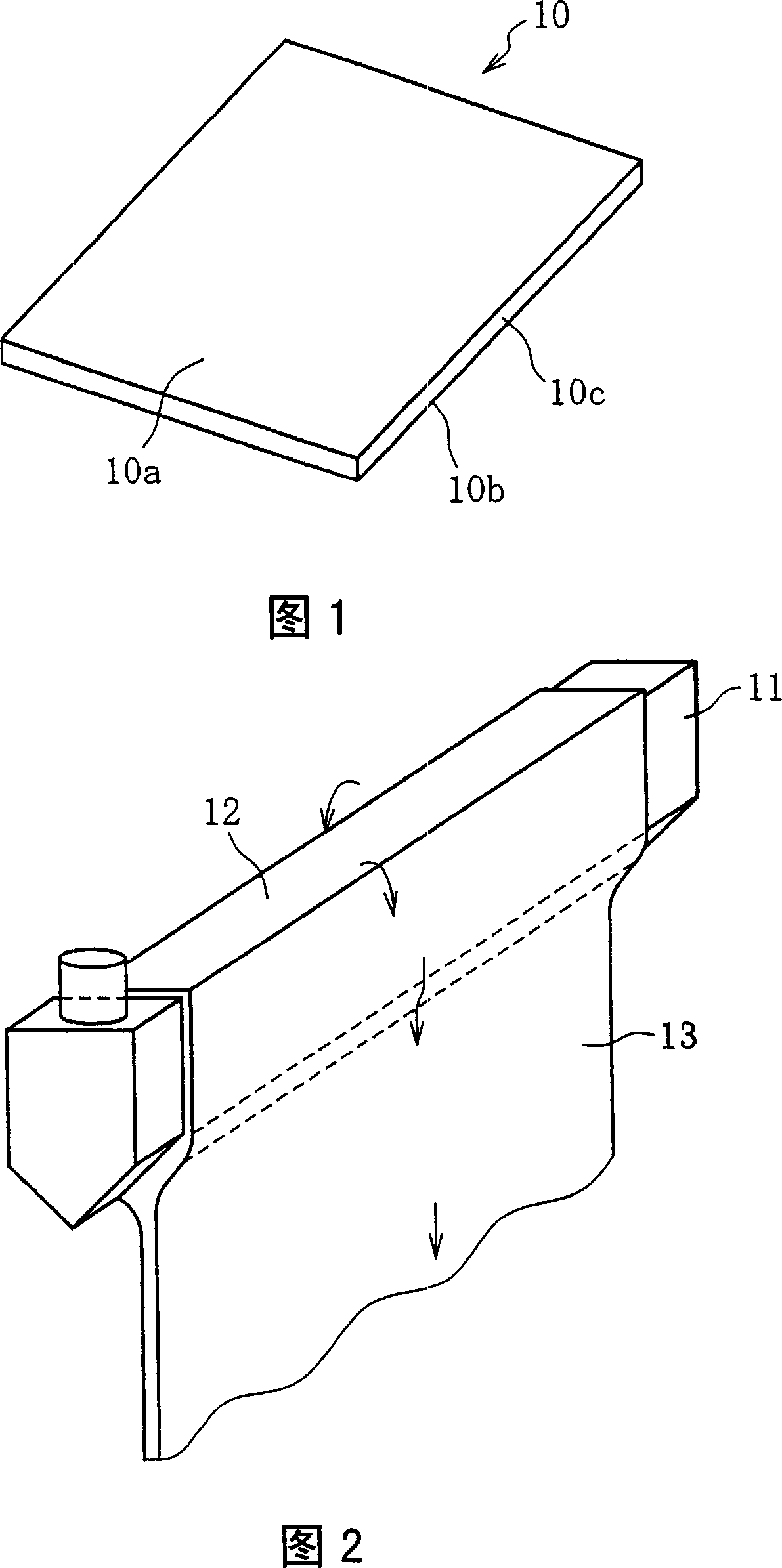
[0024] The light-transmitting surface of the cover glass for a semiconductor package of the present invention is a non-polished surface, and its surface roughness (Ra) is 1.0 nm or less. This kind of cover glass with high surface quality can be formed by down-draw method or float method. As the down-draw method, although the overflow down-draw method or the slit down-draw method is suitable, especially for the case of the overflow down-draw method, since the glass surface is a free surface and does not come into contact with other members, by controlling the melting conditions or forming conditions, it is possible to obtain It has a desired thickness (0.05-0.7 mm in the case of a cover glass for a semiconductor package) and is excellent in surface smoothness, and is therefore preferable. That is, when the overflow down-draw method is used, since the surface (light-transmitting surface) can not be ground to obtain a smooth surface, it is possible to produce a surface roughness ...
PUM
| Property | Measurement | Unit |
|---|---|---|
| surface roughness | aaaaa | aaaaa |
| thickness | aaaaa | aaaaa |
| density | aaaaa | aaaaa |
Abstract
Description
Claims
Application Information