Method of manufacturing semiconductor device

A manufacturing method and semiconductor technology, applied in semiconductor/solid-state device manufacturing, semiconductor devices, electric solid-state devices, etc., can solve problems such as deterioration of storage element operating characteristics, difficult to achieve withstand voltage of MOS transistors, and excessive thickness of tunnel insulating film, etc. Achieve the effect of preventing reverse tunnel failure and inhibiting malfunction

Inactive Publication Date: 2007-04-11
SANYO ELECTRIC CO LTD
View PDF2 Cites 2 Cited by
  • Summary
  • Abstract
  • Description
  • Claims
  • Application Information

AI Technical Summary

Problems solved by technology

Therefore, considering the operation characteristics (threshold voltage, storage current value, etc.)
In the conventional manufacturing method, as described above, since the manufacturing process of the tunnel insulating film and the gate insulating film of the MOS transistor are the same, it is ideal in that the manufacturing process can be simplified. However, in order to make the MOS transistor high Withstanding voltage, when the film thickness of the gate insulating film is increased, the thickness of the tunnel insulating film of the memory transistor becomes too thick at the same time, and the operating characteristics of the memory element deteriorate

Method used


Image

  • Method of manufacturing semiconductor device
  • Method of manufacturing semiconductor device
  • Method of manufacturing semiconductor device

Examples


Embodiment Construction

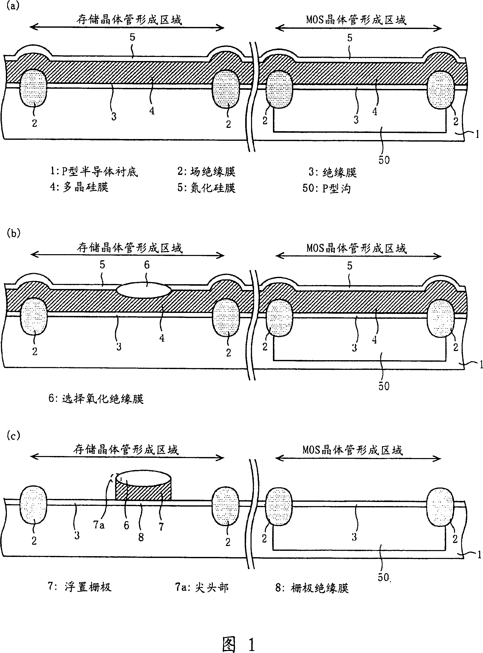
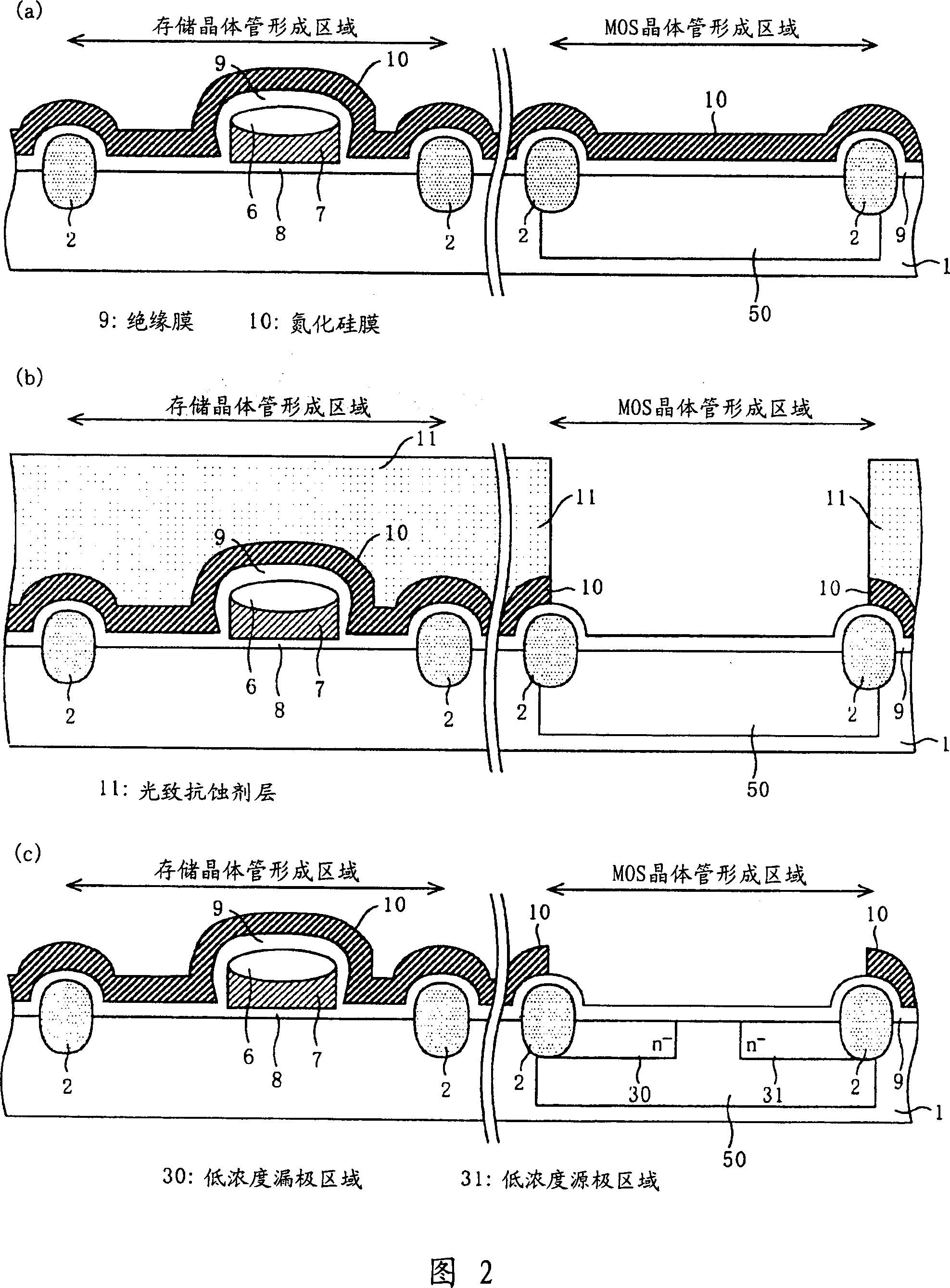
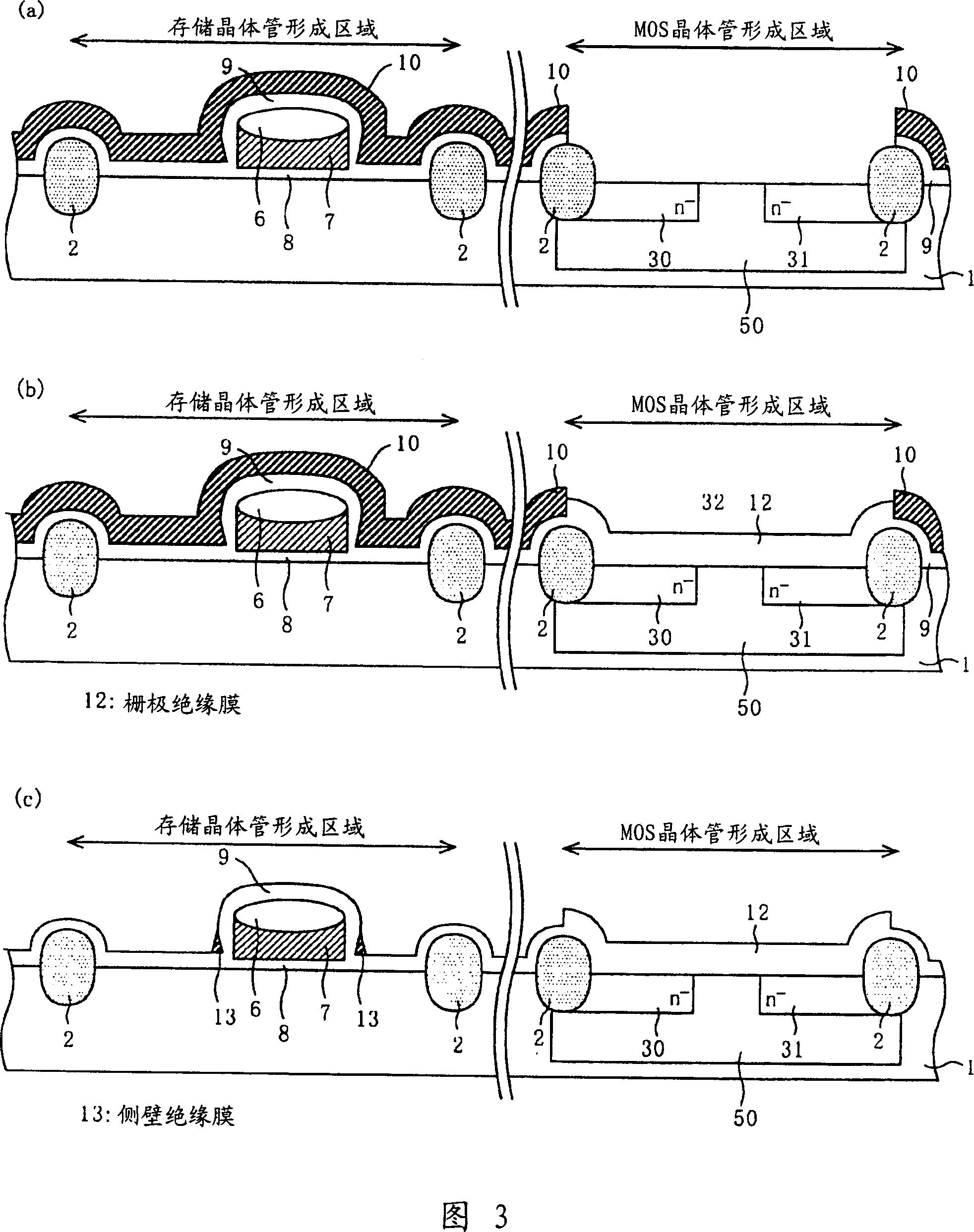
[0068] Next, a method of manufacturing a semiconductor device according to an embodiment of the present invention will be described with reference to the drawings. In addition, in the following description, an example of applying the present invention to a method of manufacturing a semiconductor device made of a P-type semiconductor substrate is introduced, but the present invention can also be applied to a method of manufacturing a semiconductor device made of an N-type semiconductor substrate. . In addition, in FIGS. 1 to 5 , the memory transistor formation region is formed on the left side, and the N-channel MOS transistor formation region is formed on the right side.

[0069] First, as shown in FIG. 1( a ), P-type impurities (boron) are ion-implanted into the surface of the P-type semiconductor substrate 1 in the MOS transistor formation region to form a P-type trench 50 . Then, on the surface of the semiconductor substrate 1, a field insulating film 2 having a film thick...


PUM


Abstract

A memory transistor and a high breakdown voltage MOS transistor are easily formed on the same semiconductor substrate without changing the operational characteristics of the memory transistor. The process of forming the tunnel insulation film of the memory transistor and the process of forming the gate insulation film of the MOS transistor are performed separately. Concretely, an insulation film to be a part of the tunnel insulation film and a silicon nitride film are formed on the whole surface, and then the silicon nitride film in a MOS transistor formation region is selectively removed using a photoresist layer. Then, the MOS transistor formation region is selectively oxidized using the remaining silicon nitride film as an anti-oxidation mask to form the gate insulation film of the MOS transistor having a selected thickness.

Description

technical field [0001] The present invention relates to a method of manufacturing a semiconductor device, and more particularly to a method of manufacturing a semiconductor device including a split-gate nonvolatile memory transistor and a MOS transistor. Background technique [0002] In recent years, an electrically erasable and program-readable dedicated storage device (hereinafter referred to as EEPROM) has been widely used as a flash memory due to the expansion of application fields such as mobile phones and digital cameras. [0003] EEPROM stores multi-valued digital data of two or more values ​​by whether a specified amount of charge is stored in the floating gate (floating gate), and by detecting the conduction change of the channel region corresponding to the amount of charge, Digital data can be read. [0004] The EEPROM is classified into: a stacked-gate type (Stacked-Gate Type) having a structure in which a floating gate and a control gate are sequentially stacked...

Claims


Application Information

Patent Timeline
Patent Type & Authority Applications(China)
IPC IPC(8): H01L21/8247H01L21/283H01L21/316H01L21/32
CPCH01L21/823462H01L21/823456H01L27/11526H01L27/1052H01L29/7883H01L29/42324H01L27/11536H01L27/105H01L21/8239H10B41/44H10B41/40H10B99/00
Inventor 饭田伊豆雄
Owner SANYO ELECTRIC CO LTD
Why Eureka
Try Eureka