

Semiconductor device
A semiconductor and device technology, applied in the field of semiconductor devices, can solve the problems of low storage capacity of pattern memory, small total number of test steps, short test time, etc., and achieve high efficiency
- Summary
- Abstract
- Description
- Claims
- Application Information
AI Technical Summary
Problems solved by technology
Method used
Image

Examples
no. 1 example approach
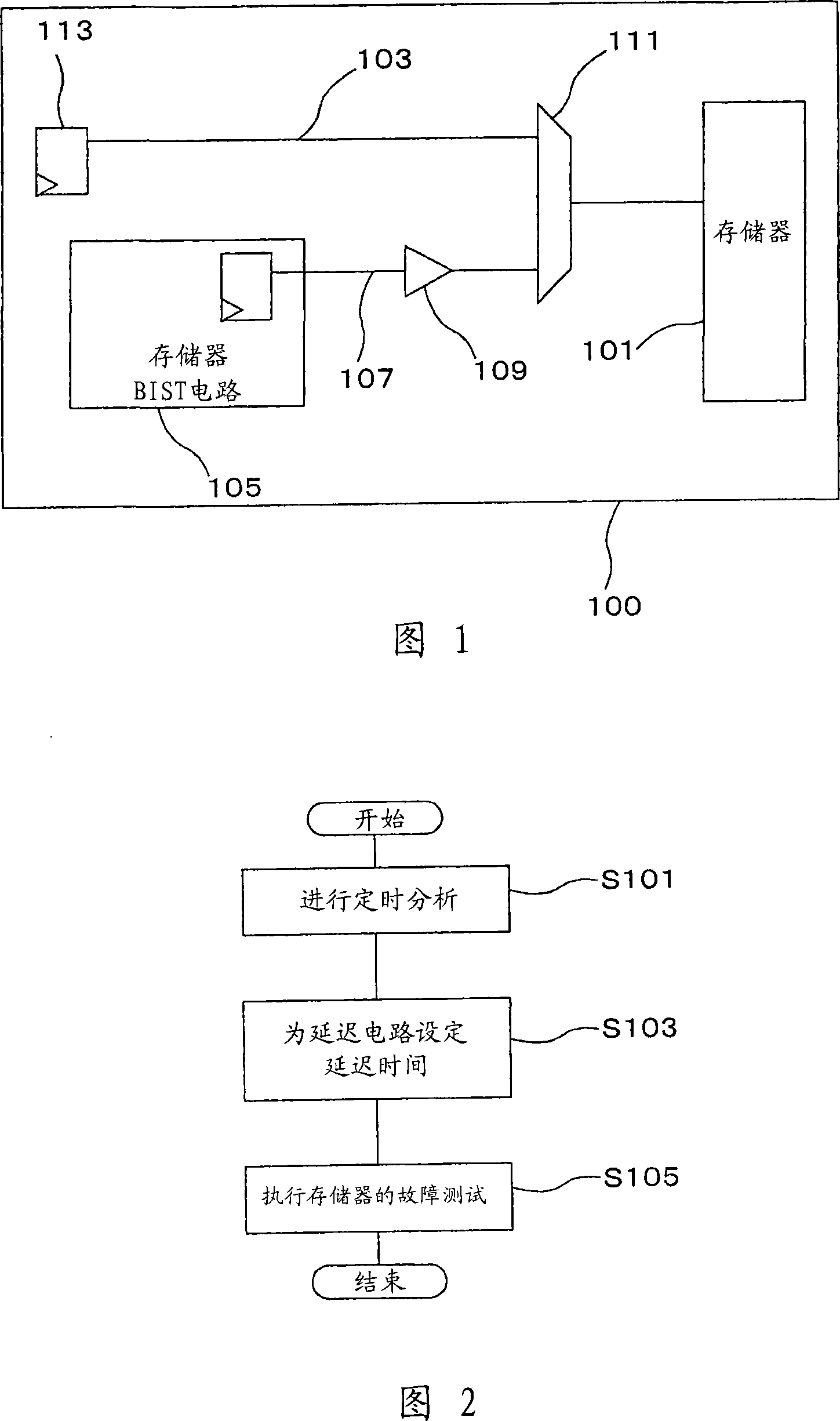
[0024] FIG. 1 is a block diagram for showing the structure of a semiconductor device 100 according to a first embodiment mode of the present invention. As shown in FIG. 1, the semiconductor device 100 of the first embodiment mode is an LSI (Large Scale Integration), which is equipped with a memory 101, a normal operation path 103, a memory BIST (built-in self-test) circuit 105, a test operation path 107 , a delay circuit 109 , and a selector 111 . The LSI has a function for self-testing the memory 101 .
[0025] The normal operation path 103 is within the semiconductor device 100 and corresponds to a critical path defined from a flip-flop (FF) 113 of a data processing unit (not shown) to the memory 101 . The memory BIST circuit 105 performs timing analysis (STA) of the normal operation path 103, generates a test pattern, and performs a failure test for the memory 101 by using the generated test pattern. This test operation path 107 corresponds to the path defined from the me...
no. 2 example approach
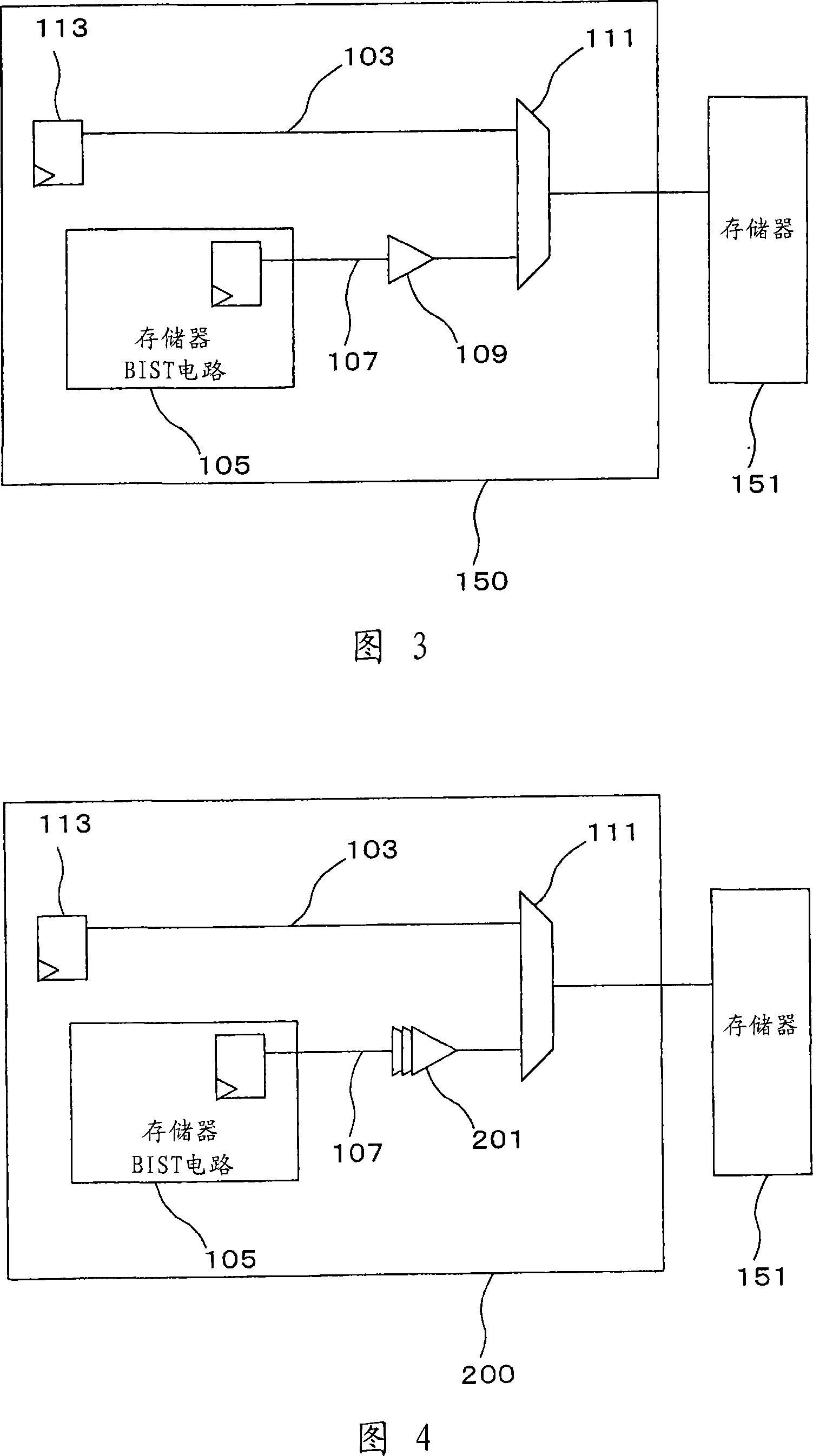
[0031] FIG. 4 is a block diagram for showing the structure of a semiconductor device 200 according to a second embodiment mode of the present invention. The semiconductor device 200 of this second embodiment mode differs from the semiconductor device 100 as described in the first embodiment mode in the following points. That is, in the second embodiment mode, the memory 151 is provided outside the semiconductor device 200, and the delay value set to the delay circuit 201 is variable. Except for the above points, other points are similar to those in the first embodiment mode, and the same reference numerals shown in FIG. 1 have been used as those for explaining commonly used structural elements shown in FIG. 4 . Since the delay amount of the delay circuit 201 is variable, the performance of the normal operation path 103 can be evaluated.
[0032] It should also be noted that the delay circuit 201 of the second embodiment mode may alternatively include a fuse (not shown) in wh...
no. 3 example approach
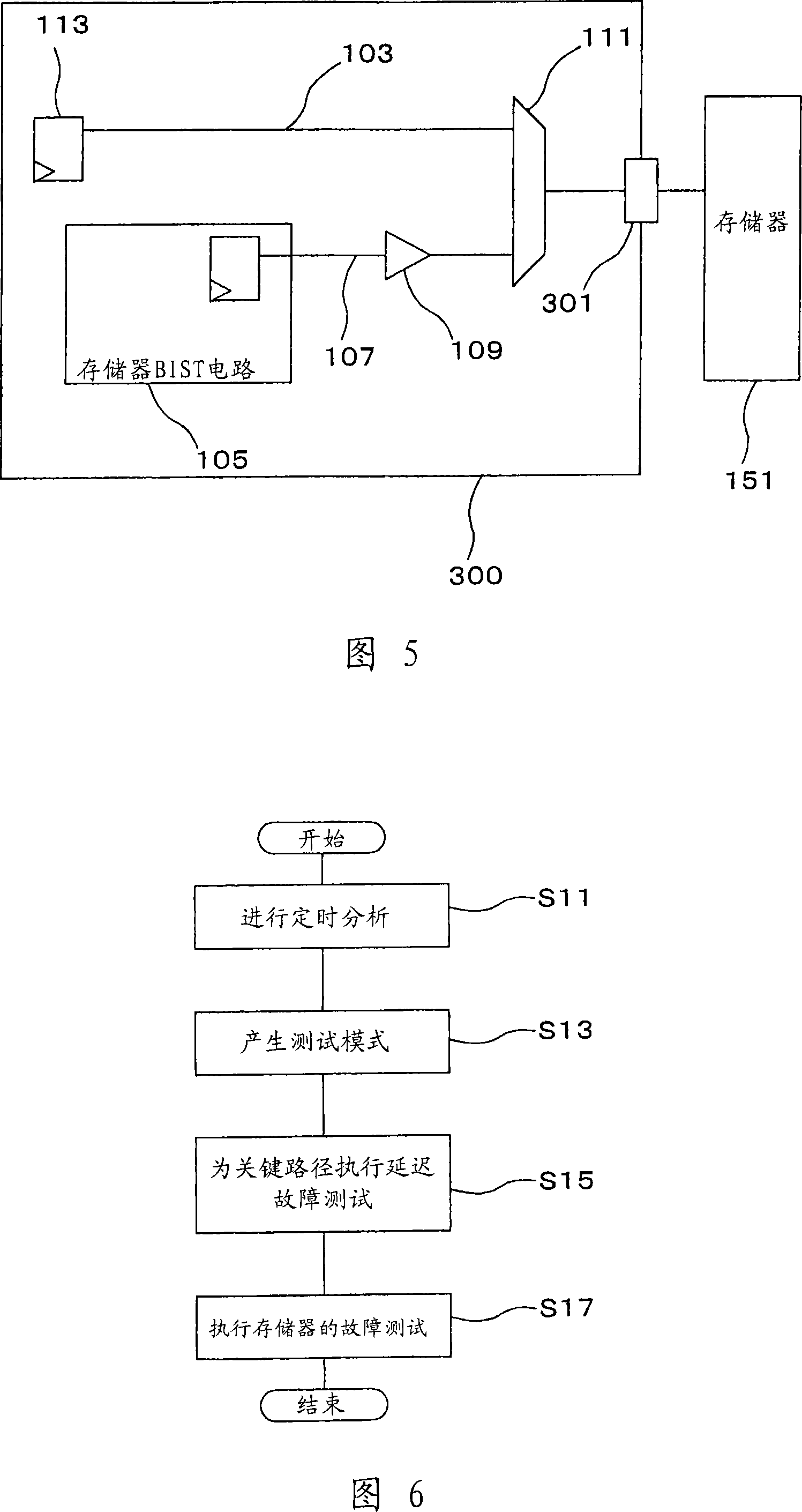
[0034] FIG. 5 is a block diagram for showing the structure of a semiconductor device 300 according to a third embodiment mode of the present invention. The semiconductor device 300 of this third embodiment differs from the semiconductor device 100 described in the first embodiment in the following points. That is, in the third embodiment mode, the memory 151 is provided outside the semiconductor device 300 , and the output terminal 301 of the semiconductor device 300 is provided at the output terminal of the selector 111 . The output terminal 301 is connected to the externally provided memory 151 . Except for the above points, other points are similar to those in the first embodiment mode, and the same reference numerals shown in FIG. 1 have been used as those for explaining commonly used structural elements shown in FIG. 5 . The output terminal 301 has a circuit (not shown) that switches the current level of each signal output from the selector 111 . Alternatively, the ext...
PUM
 Abstract
Description
Claims
Application Information