Method for fabricating semiconductor device
A manufacturing method and semiconductor technology, applied in semiconductor/solid-state device manufacturing, microstructure devices, manufacturing microstructure devices, etc., can solve problems such as damage and achieve the effect of inhibiting damage
- Summary
- Abstract
- Description
- Claims
- Application Information
AI Technical Summary
Problems solved by technology
Method used
Image

Examples
no. 1 example
[0065] Hereinafter, a method of manufacturing a semiconductor device according to a first embodiment of the present invention will be described with reference to the drawings.
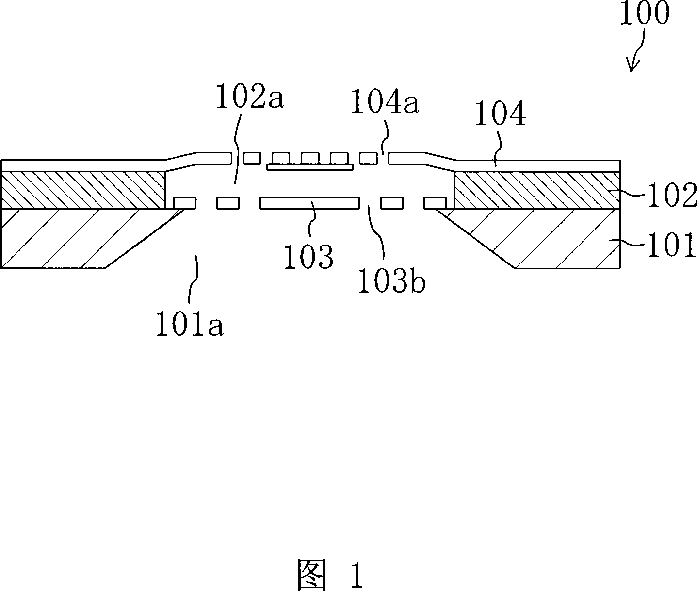
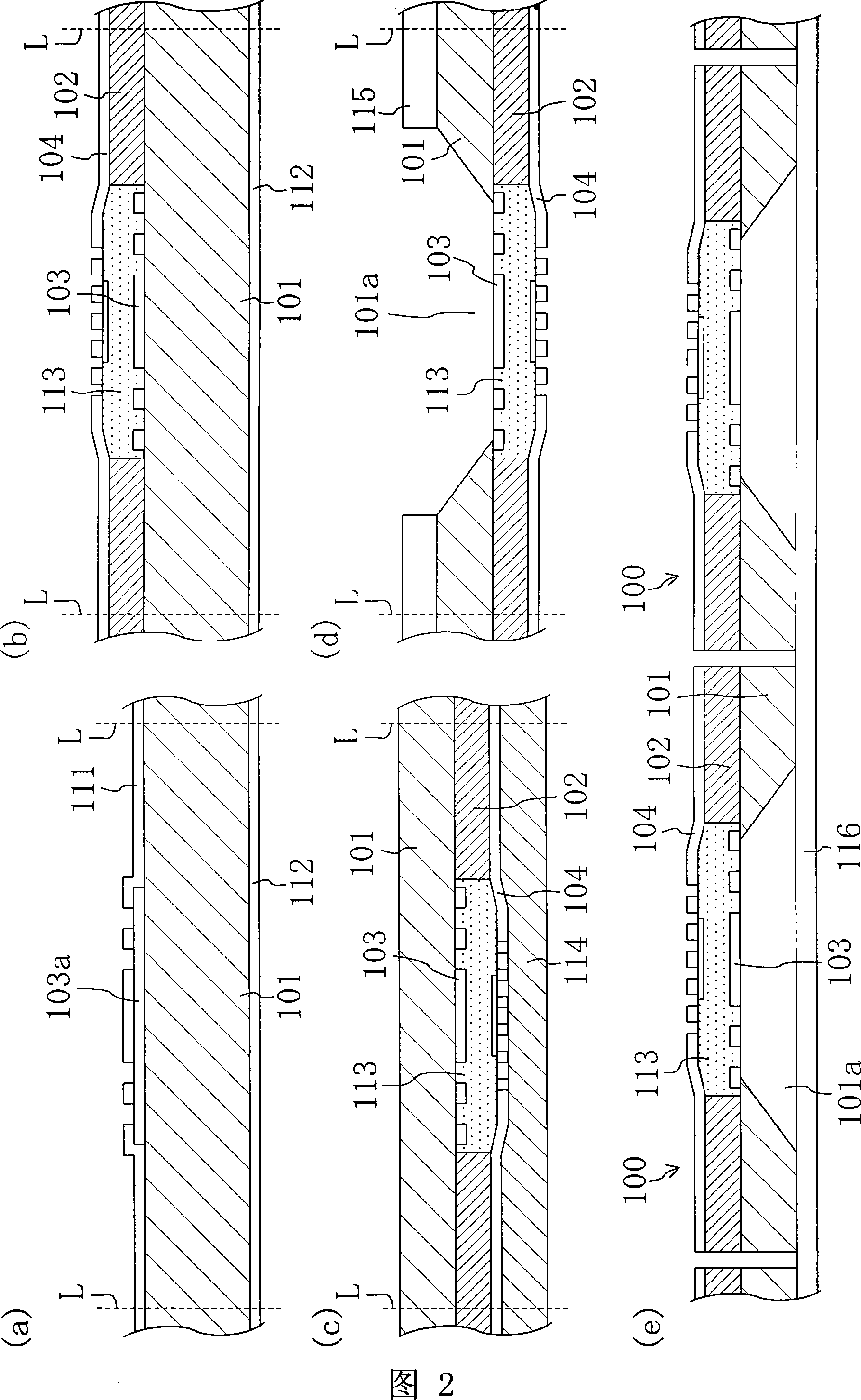
[0066] FIG. 2( a ) to FIG. 2( e ) show the manufacturing method of the MEMS microphone chip 100 of this embodiment.
[0067] First, as shown in FIG. 2( a ), a laminated material film 103 a for processing into the vibrating membrane 103 is formed on one surface (hereinafter referred to as the surface) of the semiconductor wafer 101 . The laminated material film 103a can be formed by, for example, laminating a silicon nitride (SiN) film, a polysilicon (PS: Poly Silicon) film, a tetraethylorthosilicate (TEOS: Tetraetylorthosilicate) film, and a SiN film sequentially from bottom to top. Structure.
[0068] Next, what is formed to cover the laminated material film 103a and has a pattern corresponding to the processed shape of the vibrating film 103 is, for example, silicon dioxide (SiO 2 ) film etch stop ...
no. 2 example
[0093] Next, a method of manufacturing a semiconductor device according to a second embodiment of the present invention will be described with reference to the drawings. In this embodiment, the MEMS microphone chip 100 shown in FIG. 1 is also taken as an example for illustration. In addition, since it is the same as the first embodiment except for the process of removing the sacrificial layer 113 and the process of forming the chip, the process of forming the chip in this embodiment will be mainly described here. In addition, FIGS. 4( a ) to 4 ( c ), and FIGS. 5( a ) and 5 ( b ) are diagrams illustrating the manufacturing process of the semiconductor device in this embodiment.
[0094] Specifically, first, the steps of Fig. 2(a) to Fig. 2(d) are performed in the same manner as in the first embodiment. By this method, a semiconductor wafer 101 having a plurality of individual chip structures can be obtained, as shown in FIG. 2( d ).
[0095] Next, as shown in FIG. 4( a ), the...
no. 3 example
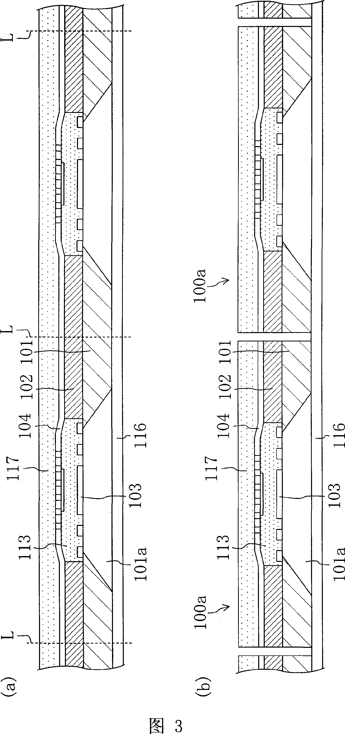
[0118] Next, a method of manufacturing a semiconductor device according to a third embodiment of the present invention will be described with reference to the drawings. In this embodiment, the MEMS microphone chip 100 shown in FIG. 1 is also taken as an example for illustration. In addition, since it is the same as the first embodiment except for the process of removing the sacrificial layer 113 and the process of forming the chip, the process of forming the chip in this embodiment will be mainly described. In addition, FIGS. 7( a ) to 7 ( c ) and FIGS. 8( a ) and 8 ( b ) are diagrams illustrating a method of manufacturing a semiconductor device according to this embodiment.
[0119] Specifically, first, the steps of Fig. 2(a) to Fig. 2(d) are performed in the same manner as in the first embodiment. In this way, as shown in FIG. 2( d ), it is possible to obtain a semiconductor wafer 101 having a structure in which a plurality of fixed films 104 are formed on the vibrating fil...
PUM
 Abstract
Description
Claims
Application Information
 - Generate Ideas
- Intellectual Property
- Life Sciences
- Materials
- Tech Scout
- Unparalleled Data Quality
- Higher Quality Content
- 60% Fewer Hallucinations
Browse by: Latest US Patents, China's latest patents, Technical Efficacy Thesaurus, Application Domain, Technology Topic, Popular Technical Reports.
© 2025 PatSnap. All rights reserved.Legal|Privacy policy|Modern Slavery Act Transparency Statement|Sitemap|About US| Contact US: help@patsnap.com