

Semiconductor component and method for manufacturing semiconductor component
A semiconductor and component technology, which is applied in the field of semiconductor components and the manufacture of semiconductor components
- Summary
- Abstract
- Description
- Claims
- Application Information
AI Technical Summary
Problems solved by technology
Method used
Image

Examples
Embodiment Construction
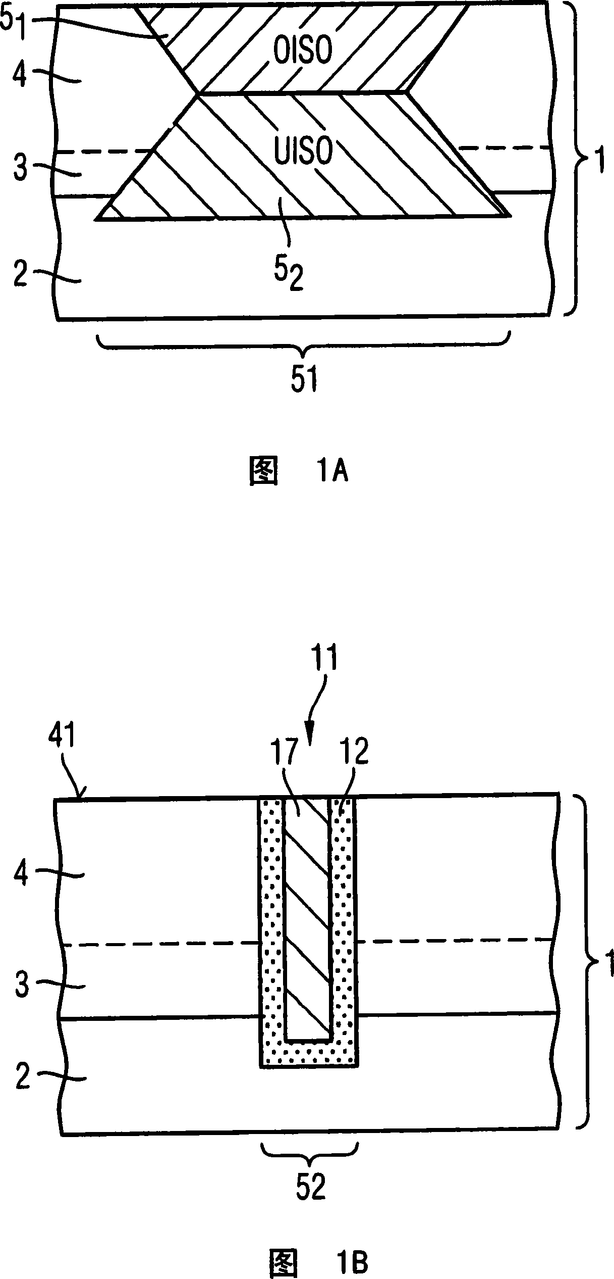
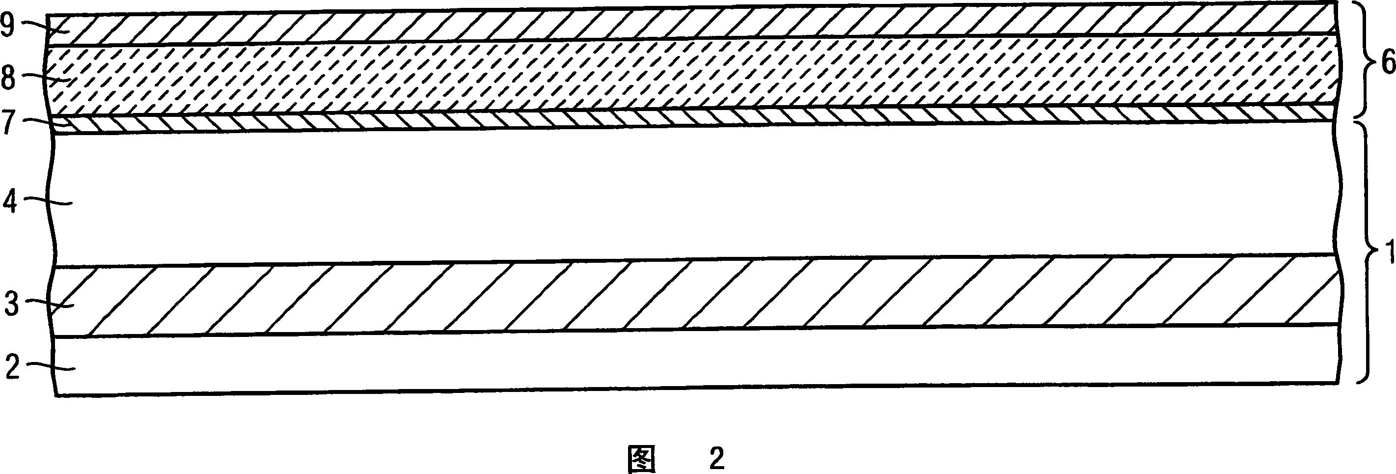
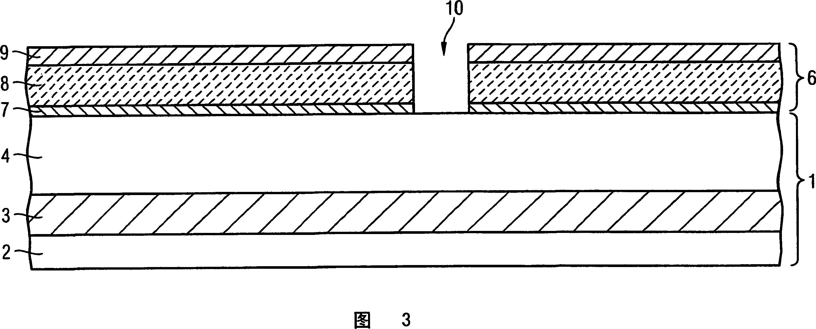
[0048] In the following detailed description, reference is made to the accompanying drawings, which constitute a part of this specification, and in which are shown by way of illustrations specific embodiments in which the invention may be practiced. In this regard, directional terms such as "top", "bottom", "front", "rear", "leading", "trailing", etc., are used with reference to the orientation of the depicted figures. Since components of embodiments of the present invention may be positioned in many different orientations, directional terms are used for purposes of illustration only and are in no way limiting. It is to be understood that other embodiments may be utilized and structural or logical changes may be made without departing from the scope of the present invention. Accordingly, the following detailed description is not to be taken in a limiting sense, and the scope of the invention will be defined by the appended claims.
[0049] In the figures, identical or mutuall...
PUM
 Abstract
Description
Claims
Application Information