Preparation method of static random access memory

A static random access memory technology, applied in semiconductor/solid state device manufacturing, electric solid state devices, semiconductor devices, etc., can solve problems such as voltage mismatch of static random access memory

Active Publication Date: 2021-04-09
晶芯成(北京)科技有限公司
View PDF7 Cites 3 Cited by
  • Summary
  • Abstract
  • Description
  • Claims
  • Application Information

AI Technical Summary

Problems solved by technology

[0006] The purpose of the present invention is to provide a preparation method of SRAM to solve the problem of voltage mismatch of SRAM

Method used


Image

  • Preparation method of static random access memory
  • Preparation method of static random access memory
  • Preparation method of static random access memory

Examples


preparation example Construction

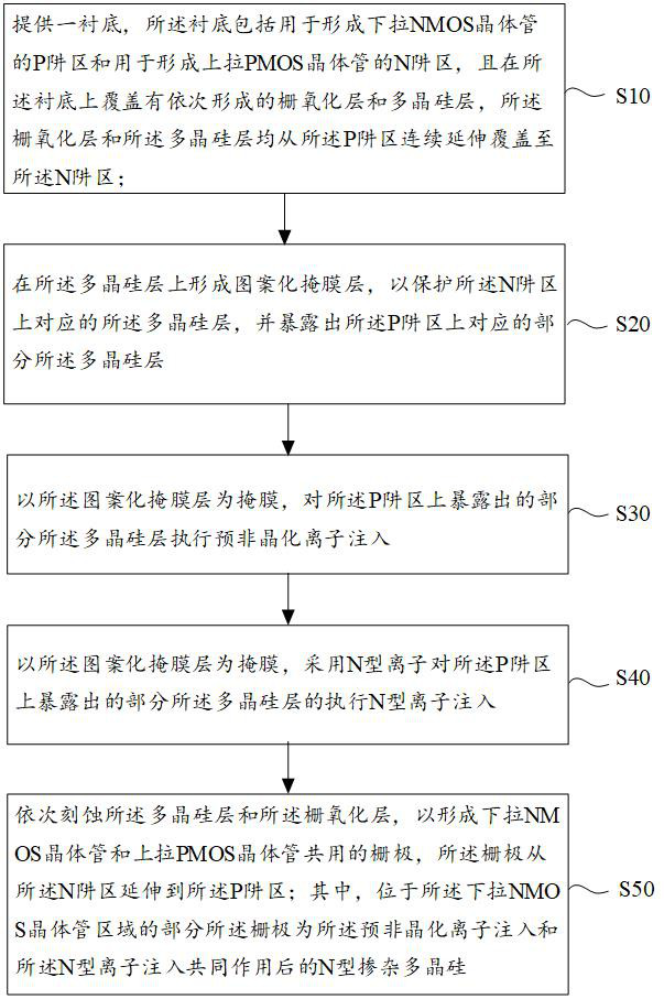
[0031] In order to solve the above technical problems, this embodiment provides a preparation method of SRAM, please refer to figure 2 , the preparation method of the SRAM comprises:

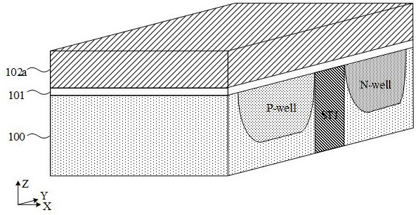
[0032] Step 1 S10: providing a substrate, the substrate includes a P well region for forming a pull-down NMOS transistor and an N well region for forming a pull-up PMOS transistor, and the substrate is covered with sequentially formed gates An oxide layer and a polysilicon layer, both of the gate oxide layer and the polysilicon layer continuously extend from the P well region to cover the N well region.

[0033] Step 2 S20: forming a patterned mask layer on the polysilicon layer to protect the corresponding polysilicon layer on the N well region and expose a corresponding part of the polysilicon layer on the P well region.

[0034] Step 3 S30: Using the patterned mask layer as a mask, performing pre-amorphization ion implantation on the exposed part of the polysilicon layer on the P well regio...


PUM


Abstract

The invention provides a preparation method of a static random access memory. According to the preparation method, pre-amorphization ion implantation is performed on a part of a polycrystalline silicon layer before N-type ion implantation is performed, so that the condition that implanted ions longitudinally diffuse, penetrates a gate oxide layer and enters a P well region due to overlarge grain size in the polycrystalline silicon layer in the N-type ion implantation process can be prevented, so that the reduction of the threshold voltage of a subsequently formed pull-down NMOS transistor caused by the above condition can be avoided, and the voltage mismatch can be avoided; meanwhile, the inhibition effect of N-type ion implantation on a polycrystalline depletion effect is improved; and besides, a pull-up PMOS transistor and a pull-down NMOS transistor which are formed subsequently share the same gate structure, so that transverse diffusion of ions in the N-type ion implantation can be inhibited by executing the pre-amorphization ion implantation, the influence of the N-type ion implantation on the threshold voltage of the pull-up PMOS transistor formed subsequently is avoided, and the problem of voltage mismatch is relieved, and device performance can be improved. The same mask is used for two times of ion implantation, and therefore, the preparation cost is low, and the process is simple.

Description

technical field [0001] The invention relates to the technical field of semiconductor device manufacture, in particular to a preparation method of a static random access memory. Background technique [0002] Static Random-Access Memory (SRAM) has the advantages of high speed, low power consumption, and compatibility with standard processes, and is now widely used in electronic products such as computers, mobile phones, digital cameras, and multimedia players. [0003] The SRAM is composed of a plurality of SRAM units, and each SRAM unit is essentially composed of a pair of interconnected inverters. see figure 1 , figure 1 Shown is a six-transistor SRAM cell, including two pass-gate transistors W1 and W2, two pull-up transistors P1 and P2, and two pull-down transistors N1 and N2. Wherein, both P1 and P2 are PMOS transistors; N1 and N2 are both NMOS transistors. The gates of the transfer gate transistors W1 and W2 are controlled by the word line WL to determine whether the ...

Claims


Application Information

Patent Timeline
Patent Type & Authority Applications(China)
IPC IPC(8): H01L21/8244H01L21/266H01L27/11
CPCH01L21/266H10B10/12
Inventor 周儒领金起準詹奕鹏
Owner 晶芯成(北京)科技有限公司
Why Eureka
Try Eureka