

Formation method of transistor
A technology of transistors and semiconductors, applied in semiconductor/solid-state device manufacturing, electrical components, circuits, etc., can solve problems such as transistor performance needs to be improved
- Summary
- Abstract
- Description
- Claims
- Application Information
AI Technical Summary
Problems solved by technology
Method used
Image

Examples
Embodiment Construction
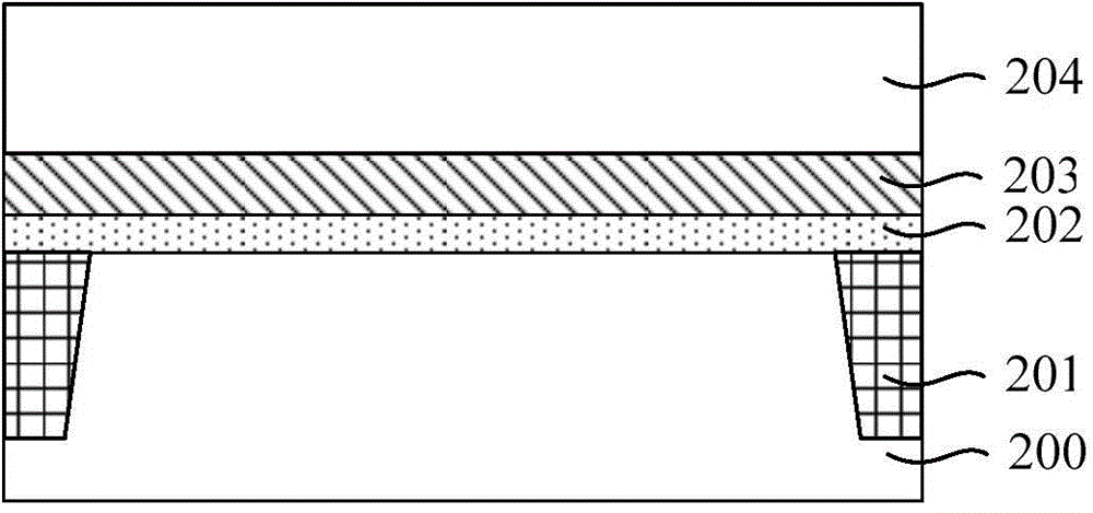
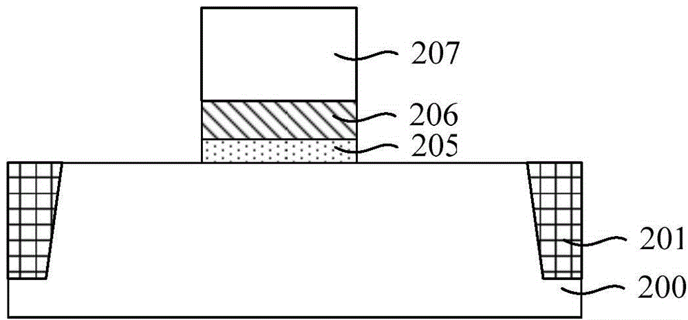
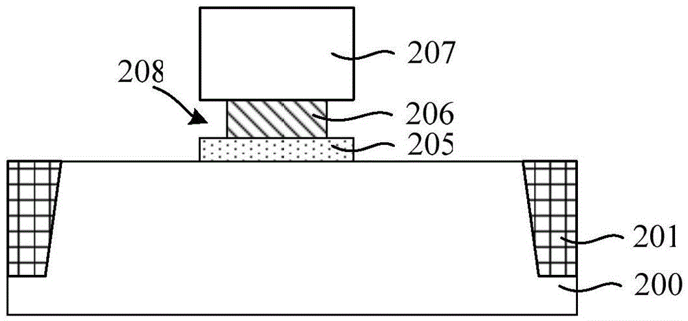
[0034] The performance of the conventionally formed transistors still needs to be improved, for example, the problem of the short channel effect still exists in the transistors formed by the prior art.
[0035] Research has found that in the prior art, there are problems of uneven ion concentration distribution and inaccurate position in the pocket implant region formed by ion implantation in the pocket implant region, especially in the parts near the bottom of the gate electrode and the channel region of the transistor. It is outstanding that the transistor still has the problem of short channel when it is working. Further studies have found that the reason for the uneven distribution of ion concentration and inaccurate positions in the pocket implantation region is that during the pocket ion implantation process, the gate electrode and offset sidewalls will affect the implanted ion beam.
[0036]To this end, the present invention provides a method for forming a transistor. A...
PUM
| Property | Measurement | Unit |
|---|---|---|
| Thickness | aaaaa | aaaaa |
| Thickness | aaaaa | aaaaa |
| Width | aaaaa | aaaaa |
Abstract
Description
Claims
Application Information