Defect detecting device and defect detecting method

A defect inspection and defect technology, which is applied in the direction of measuring devices, instruments, scientific instruments, etc., can solve the problems that the workpiece cannot be transported, and the delivery period cannot be shortened, so as to achieve the effect of shortening the delivery period

Inactive Publication Date: 2008-01-09
OLYMPUS CORP
View PDF3 Cites 12 Cited by
  • Summary
  • Abstract
  • Description
  • Claims
  • Application Information

AI Technical Summary

Problems solved by technology

[0008] In this way, conventionally, as a result of determining the transport destination (destination) of a workpiece based on defect information including lower-layer defects, the workpiece may not be transported to an appropriate transport destination.
In this case, the time for moving the workpiece in and out of the transport box and the transport time are useless, and the defect inspection is repeated during the retrospective inspection, so there is a problem that the lead time for starting the manufacturing process cannot be shortened.

Method used


Image

  • Defect detecting device and defect detecting method
  • Defect detecting device and defect detecting method
  • Defect detecting device and defect detecting method

Examples


Embodiment Construction

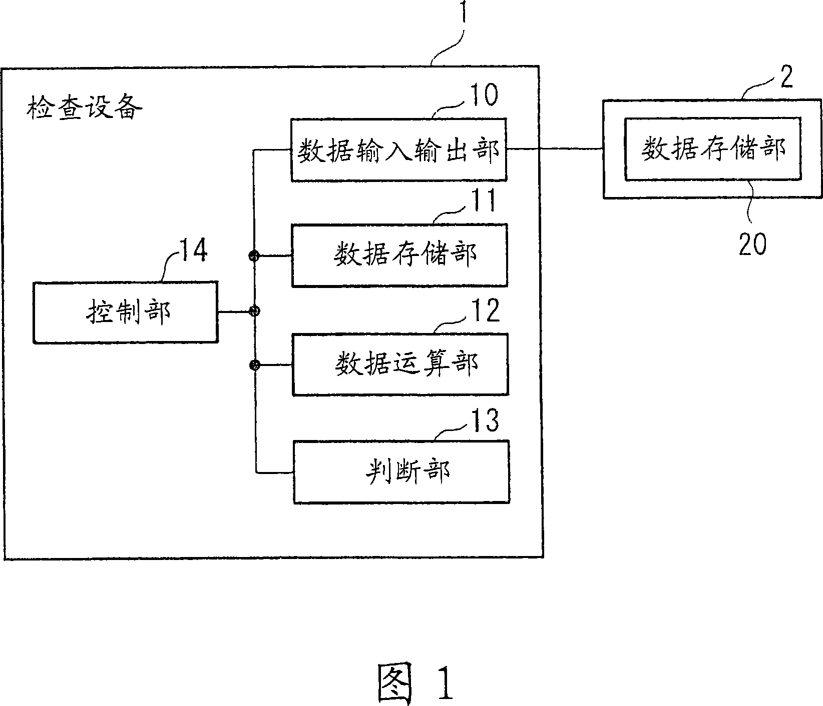
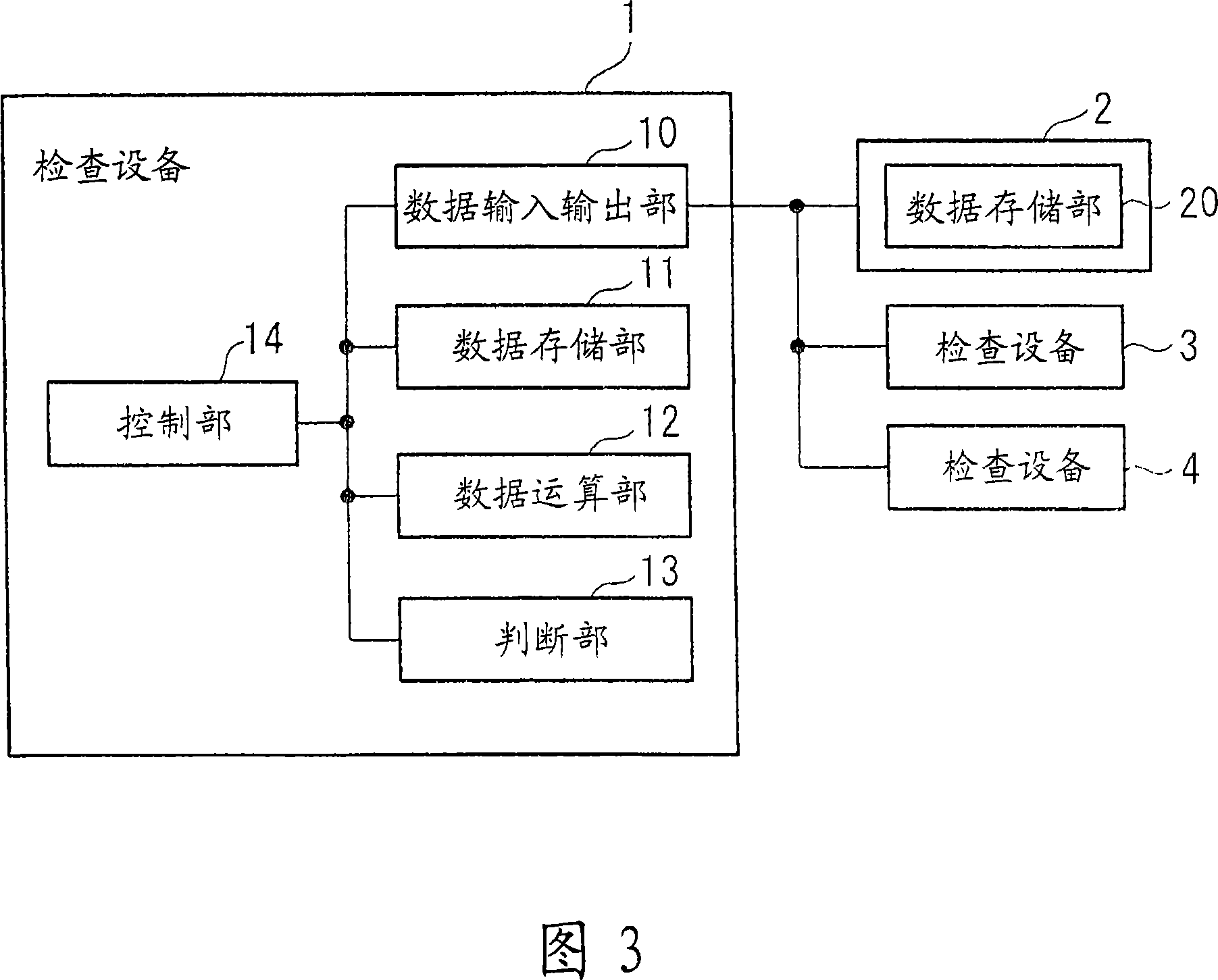
[0016] Hereinafter, preferred modes for implementing the present invention will be described with reference to the drawings. FIG. 1 is a block diagram showing the configuration of a defect inspection device according to a first embodiment of the present invention. Each structure in the drawing will be described below. The inspection device 1 is a defect inspection device that detects defects by performing macroscopic inspection or microscopic inspection on an object manufactured by sequentially laminating multiple layers on the surface by a photolithography process, such as a semiconductor wafer substrate or a glass substrate for liquid crystal display. The external device 2 is a server or the like having a data storage unit 20 which stores defect information and the like generated during inspection. The defect information includes defect position information indicating the position (coordinates) of a defect, defect type information indicating a type of defect, and the like. ...


PUM


Abstract

The invention relates to a defect inspection device and defect inspection method, which can reduce the consignment stage of manufacturing process. A control devision (14) generates defect information of identifying the defect of substrate at the time of detecting substrate. After inspecting, the control devision (14) compares the defect information of said substrate generated at the time of inspecting with defect information generated at the time of an inspection of a lower layer of said substrate. The repeated defect repeated with the defect of the lower layer is removed to generate noted-flaws information which identifies a defect generated on said top layer layer. A decision means (13) which judges a taking-out place of said substrate based on said noted-flaws information of the top layer output from the data operation part, and informs control devision (14).

Description

technical field [0001] The present invention relates to a defect inspection device and a defect inspection method for detecting defects by inspecting the appearance of an object to be inspected. This application claims priority based on Japanese Patent Application No. 2006-183112 for which it applied in Japan on July 3, 2006, and uses the content here. Background technique [0002] In the process of manufacturing (photolithography) mother glass substrates (workpieces) for liquid crystal displays, after forming a thin film on the workpiece, etc., inspections are performed for defects such as scratches, dirt adhesion, and circuit pattern defects on the surface of the workpiece. In this defect inspection, after a workpiece is loaded into the defect inspection device, the defect inspection device detects a defect on the workpiece through image processing or the like, and generates defect information including information such as a defect position for identifying the defect. Thi...

Claims


Application Information

Patent Timeline
Patent Type & Authority Applications(China)
IPC IPC(8): G01N21/956G02F1/13
CPCG01N21/8806G01N21/8851G01N21/956G01N21/958G01N2021/8858G02F1/1309
Inventor 大西孝明
Owner OLYMPUS CORP
Why Eureka
Try Eureka