Chip encapsulation structure
A chip packaging structure and chip packaging technology, which are applied in the directions of printed circuits, electrical components, and electrical solid devices connected to non-printed electrical components, can solve problems such as poor fixing, deformation of the chip packaging structure 100, poor coplanarity, etc. problem, to achieve good fixing effect, prevent falling off, and increase the effect of contact area
- Summary
- Abstract
- Description
- Claims
- Application Information
AI Technical Summary
Problems solved by technology
Method used
Image

Examples
no. 1 example
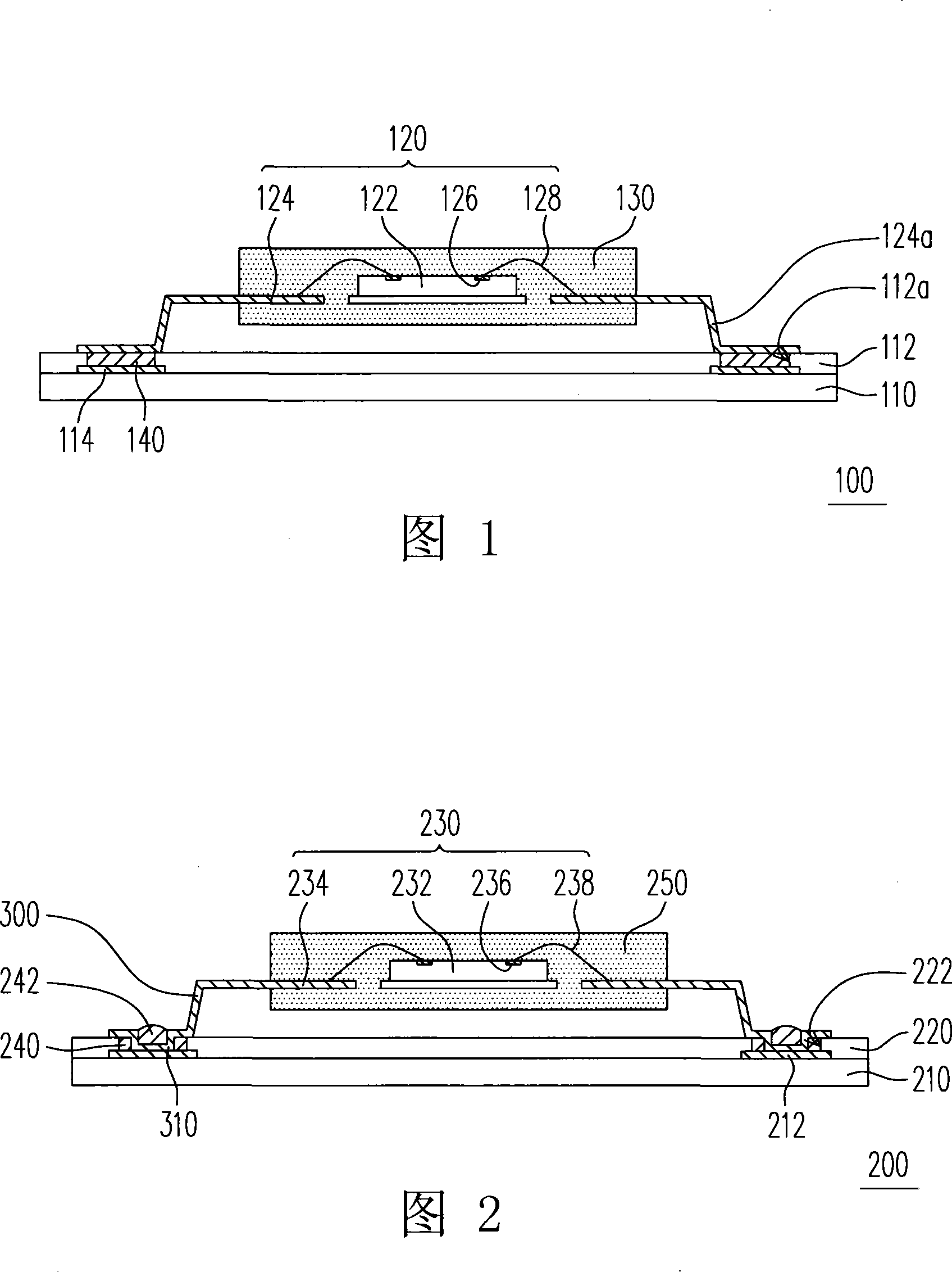
[0035] FIG. 2 is a cross-sectional view of the chip package structure in the first embodiment of the present invention. What needs to be explained first is that the circuit board has two contacts and two first openings as an example below, but the present invention is not limited thereto, and those skilled in the art can also configure only one contact on the circuit board and a first opening, or more than two contacts and the first opening are arranged.
[0036] Please refer to FIG. 2 , the chip package structure 200 includes a circuit board 210 , a solder mask 220 and a chip package 230 . The solder resist layer 220 covers the circuit board 210 , wherein the solder resist layer 220 may be formed on the circuit board 210 by screen printing, spray printing or coating. The solder resist layer 220 has a first opening 222 , and the first opening 222 exposes the contacts 212 on the circuit board 210 .
[0037] The chip package 230 includes a chip 232 and a lead frame 234 , and t...
no. 2 example
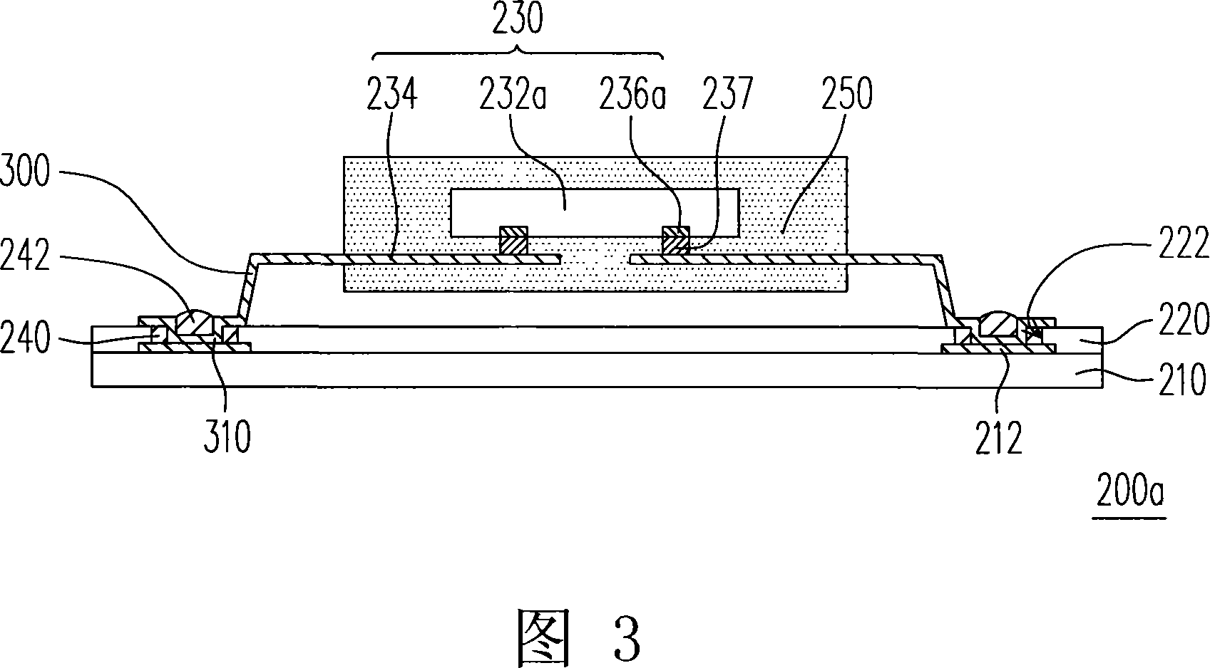
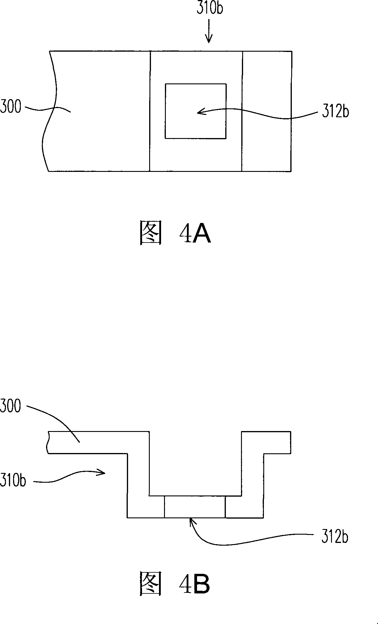
[0041] FIG. 4A is a top view of the embedded part in the second embodiment of the present invention, and FIG. 4B is a side view of the embedded part in FIG. 4A. In the second embodiment and the first embodiment, the same or similar element numbers represent the same or similar elements. The second embodiment is substantially the same as the first embodiment, and the differences between the two embodiments will be described in detail below, and the similarities will not be repeated.
[0042] Please refer to FIG. 4A and FIG. 4B , the difference between the second embodiment and the first embodiment is that the embedding portion 310 b further has a second opening 312 b. The second opening 312b can be formed by etching, or by forming the second opening 312b at the same time when the embedding portion 310b is punched, and its shape can be triangular, semicircular or semielliptical. The solder bump 240 can protrude from the second opening 312b to form the protruding portion 242, wh...
no. 3 example
[0044] Fig. 5A is a top view of the embedded part in the third embodiment of the present invention, and Fig. 5B is a side view of the embedded part in Fig. 4A. Please refer to FIG. 5A and FIG. 5B. In this embodiment, in addition to the concave cup structure shown in FIG. 4B, the embedded part can also be an arched structure as shown in FIG. 5B, and a hollow can be formed around the embedded part 310c Shaped second opening 312c and third opening 314c, while the pin 300 only retains the connecting portion 316c to be formed between the second opening 312c and the third opening 314c, and finally the connecting portion 316c is stamped into the required concave shape structure.
[0045] The shapes and manufacturing methods of the second opening 312c and the third opening 314c can refer to the above-mentioned second opening 312b, and will not be repeated here. In addition, the connecting portion 316c may also have other shapes. For example, the second opening and the third opening ...
PUM
 Abstract
Description
Claims
Application Information
 - R&D
- Intellectual Property
- Life Sciences
- Materials
- Tech Scout
- Unparalleled Data Quality
- Higher Quality Content
- 60% Fewer Hallucinations
Browse by: Latest US Patents, China's latest patents, Technical Efficacy Thesaurus, Application Domain, Technology Topic, Popular Technical Reports.
© 2025 PatSnap. All rights reserved.Legal|Privacy policy|Modern Slavery Act Transparency Statement|Sitemap|About US| Contact US: help@patsnap.com