Control method for extension slice equability for 6 inch As back lining MOS part
A technology of MOS device and control method, which is applied in semiconductor/solid-state device manufacturing, electrical components, circuits, etc., can solve the problems of unsatisfactory self-doping, unsatisfactory edge uniformity, unfavorable mass production, etc. time, the effect of reducing process time and reducing production costs
- Summary
- Abstract
- Description
- Claims
- Application Information
AI Technical Summary
Problems solved by technology
Method used
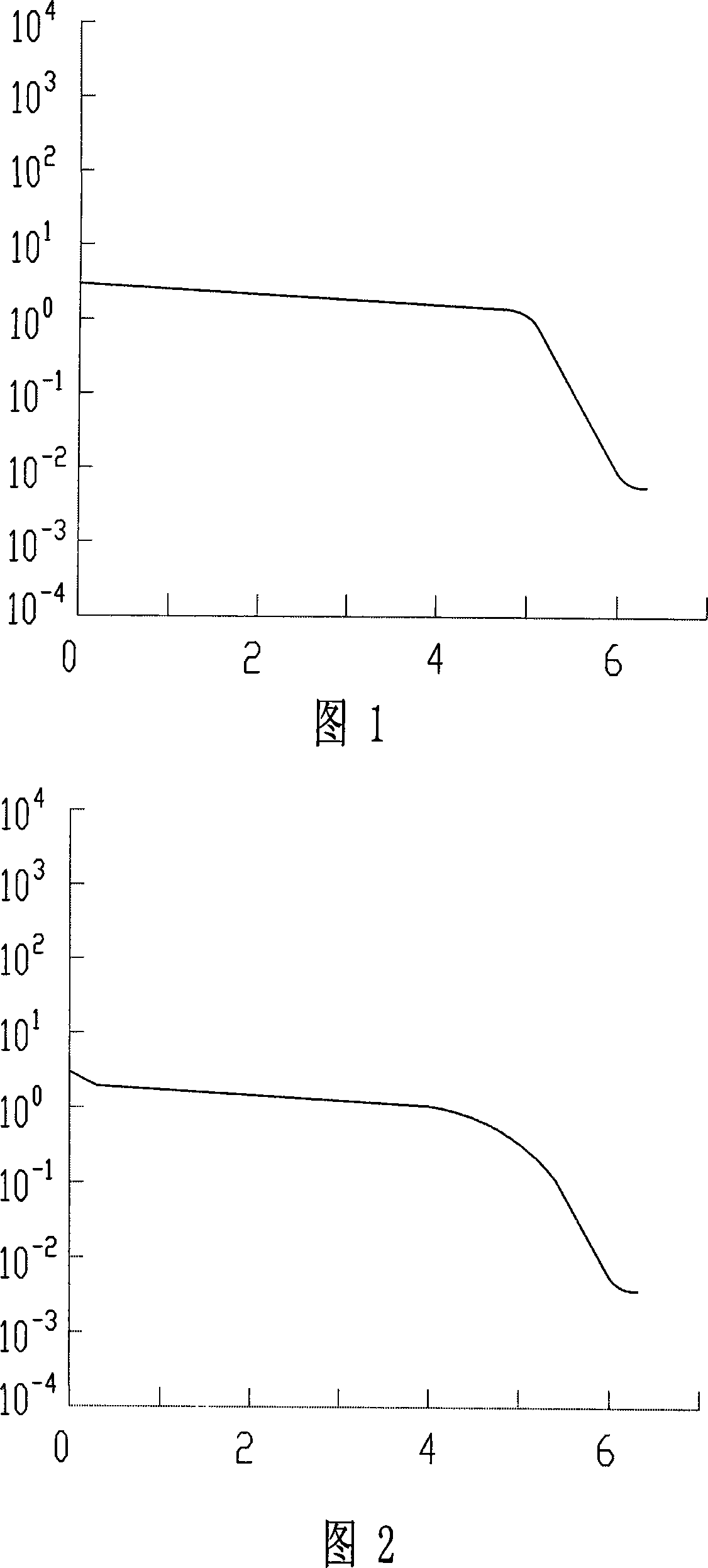
Image

Examples
Embodiment 1
[0037] 1. Substrate requirements: the following table.
[0038]
Parameter
Unit (unit)
specification
value
(standard value)
Resistivity (resistivity)
CM
0.002-0.004
RRG MAX
(resistivity radial gradient position)
%
25.0
Orientation
Degree (degree)
1-1-1
Off Orientation
(Deviation of crystal orientation)
Degree (degree)
4.0°±0.5°
Thickness and thickness
tolerance
(thickness and tolerance)
Microns (microns)
6260±20.0
Diameter and diametrical
tolerance
(diameter and tolerance)
mm (mm)
150.0+0.20
Back side
A
5000±500
[0039] 2. Extension parameters
[0040] The resistivity of the epitaxial layer is 24±8%Ω·cm, and the thickness of the epitaxial layer is 50±5%μm.
[0041] 3. The epitaxial equipmen...
Embodiment 2
[0051] The difference between this embodiment and the embodiment is that: the first time in the process 4.2 with large flow H 2 The flushing time is 30 minutes; the second time in 4.5 with large flow of H 2 Rinse and catch air for 5 minutes.
Embodiment 3
[0053] The difference between this embodiment and the embodiment is that: the first time in the process 4.2 with large flow H 2 The flushing time is 25 minutes; the second time in 4.5 with large flow of H 2 In the middle of the wash, the time is 7 minutes.
PUM
 Abstract
Description
Claims
Application Information