Method for producing substrate assembly for plasma display panel, and plasma display panel

A display panel and plasma technology, which is used in the manufacture of alternating current plasma display panels, discharge tubes/lamps, ships or lead wires, etc., can solve the problems of display quality degradation and inaccurate display, and achieve the effect of uniform formation

Inactive Publication Date: 2008-02-27
FUJITSU HITACHI PLASMA DISPLAY LTD
View PDF2 Cites 0 Cited by
  • Summary
  • Abstract
  • Description
  • Claims
  • Application Information

AI Technical Summary

Problems solved by technology

When this discharge delay increases, it will lead to various problems such as deterioration of display quality or incorrect display.

Method used


Image

  • Method for producing substrate assembly for plasma display panel, and plasma display panel
  • Method for producing substrate assembly for plasma display panel, and plasma display panel

Examples


Embodiment Construction

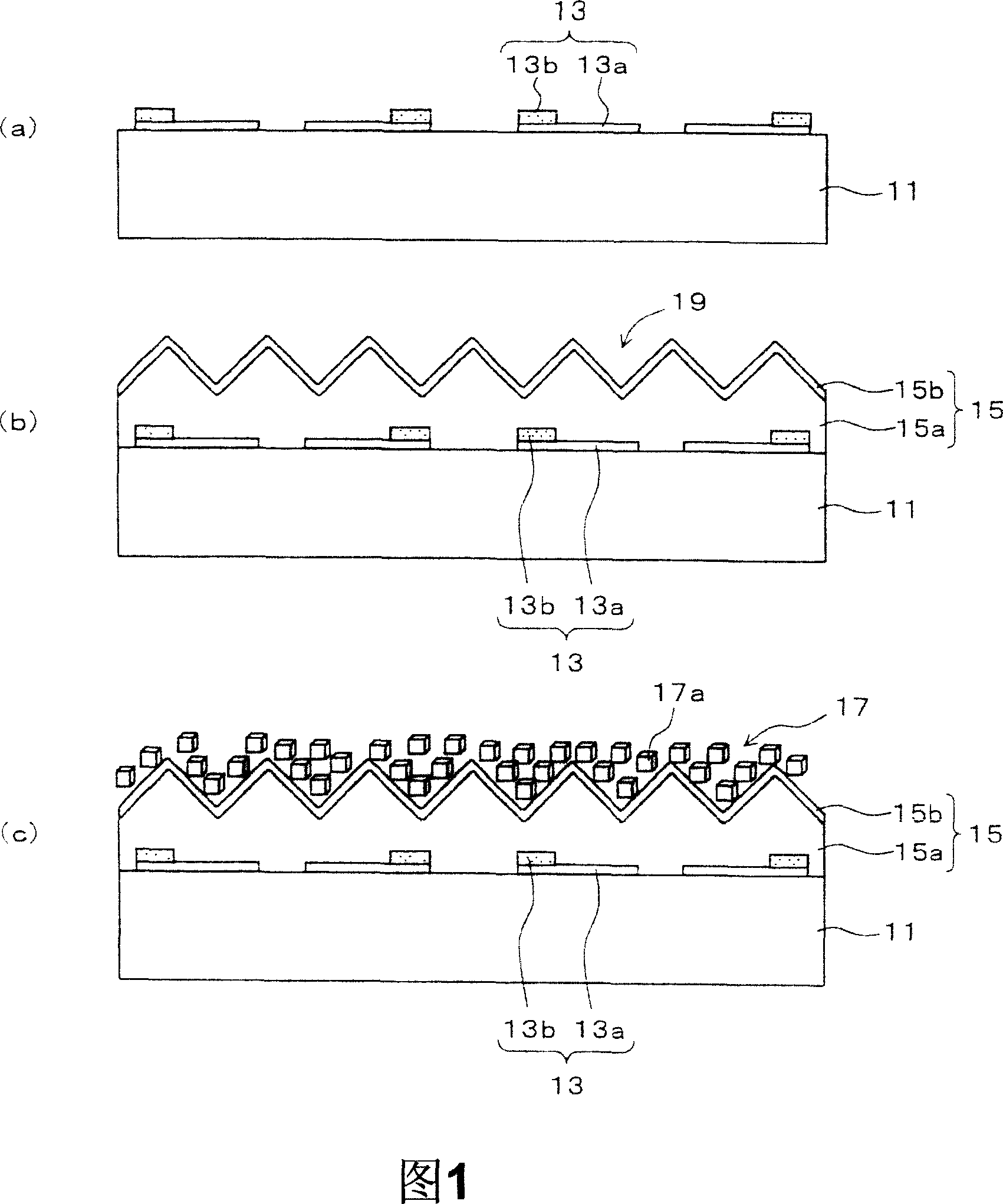
[0017] Hereinafter, embodiments of the present invention will be described with reference to the drawings. The structures shown in the drawings and the following descriptions are examples, and the scope of the present invention is not limited to those shown in the drawings and the following descriptions.

[0018] In the following embodiments, the case where the display electrodes, dielectric layer, magnesium oxide crystal layer, etc. are provided on the front side substrate structure is described as an example, but the display electrodes, dielectric layer, magnesium oxide crystal layer, etc. are provided on the back side. The situation on the substrate structure is also applicable to the present invention.

[0019] A method of manufacturing a front-side substrate structure for a PDP according to an embodiment of the present invention will be described with reference to FIGS. 1( a ) to ( c ). 1( a ) to ( c ) are cross-sectional views showing the manufacturing steps of the fron...


PUM

PropertyMeasurementUnit
particle sizeaaaaaaaaaa

Abstract

A method for producing a substrate assembly for a plasma display panel includes the steps of applying a suspension to a dielectric layer covering display electrodes formed on a substrate, the suspension containing a dispersion medium and a large number of magnesium oxide crystals dispersed in the dispersion medium, and thereafter evaporating the dispersion medium to form a layer of the magnesium oxide crystals on the dielectric layer, wherein the dielectric layer has a rugged surface structure having uniformly-dispersed projections and depressions, the rugged surface structure being capable of trapping the magnesium oxide crystals.

Description

technical field [0001] The present invention relates to a method of manufacturing a substrate structure for a plasma display panel (hereinafter referred to as "PDP") and a PDP. Background technique [0002] FIG. 2 is a three-dimensional schematic diagram of a conventional PDP structure. The PDP employs a structure in which a front-side substrate structure 1 and a rear-side substrate structure 2 are bonded together. In front-side substrate structure 1 , display electrodes 3 including transparent electrodes 31 and bus electrodes 32 are arranged on front-side substrate 1 a made of a glass substrate, and display electrodes 3 are covered with dielectric layer 4 . On the dielectric layer 4, a protective layer 5 including a magnesium oxide layer having a high secondary electron emission coefficient is further formed. On the back side substrate structure 2, the address electrodes 6 perpendicular to the display electrodes are disposed on the back side substrate 2a made of a glass s...

Claims


Application Information

Patent Timeline
Patent Type & Authority Applications(China)
IPC IPC(8): H01J9/00H01J17/02H01J17/49H01J11/00H01J9/02H01J11/12H01J11/22H01J11/24H01J11/26H01J11/34H01J11/36H01J11/38H01J11/40H01J11/42H01J11/50
CPCH01J11/40G09G3/298H01J9/02H01J11/12G09G2300/0426H01J11/38H01J9/24
Inventor 三泽智也笠原滋雄
Owner FUJITSU HITACHI PLASMA DISPLAY LTD
Why Eureka
Try Eureka