Insulated gate semiconductor device and method for manufacturing the same

一种绝缘栅型、制造方法的技术,应用在半导体/固态器件制造、半导体器件、晶体管等方向,能够解决导通特性恶化、不能够抑制二极管正向电压上升等问题,达到提高导通特性、抑制正向电压Vf、抑制恢复电流的上升的效果

Inactive Publication Date: 2008-03-05
MITSUBISHI ELECTRIC CORP
View PDF1 Cites 13 Cited by
  • Summary
  • Abstract
  • Description
  • Claims
  • Application Information

AI Technical Summary

Problems solved by technology

[0022] However, in the above-mentioned structure, the region where the IGBT is formed is only the above-mentioned group of grooves, so the diode region cannot be made sufficiently large.
Therefore, even if the gate is turned on, the rise of the diode forward voltage Vf cannot be suppressed.
In addition, in this structure, compared with the case where the IGBT and the diode are manufactured separately, the conduction characteristic deteriorates

Method used


Image

  • Insulated gate semiconductor device and method for manufacturing the same
  • Insulated gate semiconductor device and method for manufacturing the same
  • Insulated gate semiconductor device and method for manufacturing the same

Examples


Embodiment approach 1

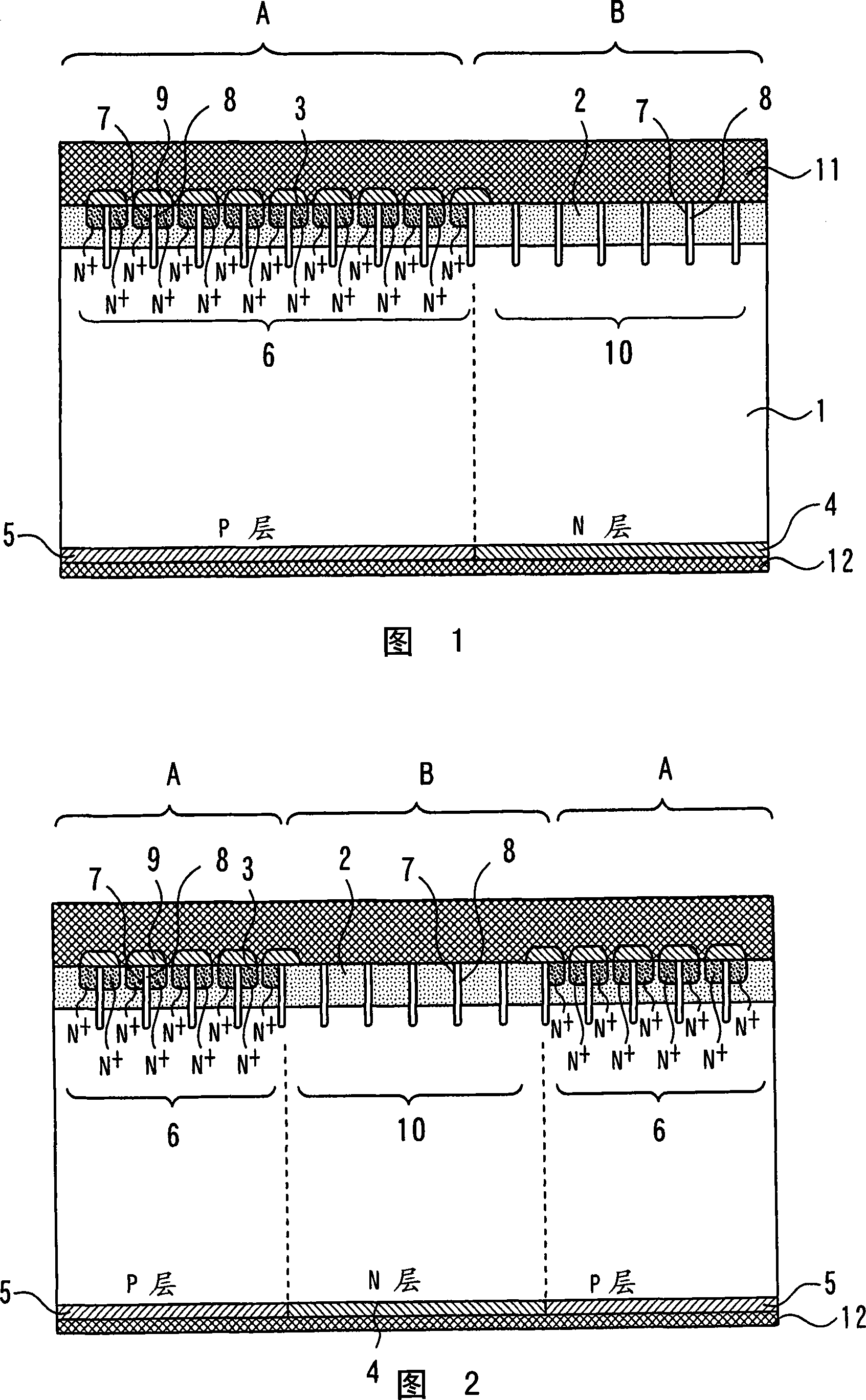
[0070] FIG. 1 shows a cross-sectional view of an insulated gate semiconductor device according to Embodiment 1. As shown in FIG. Using N with N-type impurities - substrate 1 forming the semiconductor device, N - The substrate 1 has a first main surface (upper main surface) and a second main surface (lower main surface). N - The substrate 1 has at least one region A (first region), and a region B (second region) is provided adjacent thereto. The emitter layer 3 is provided on the region A, while the emitter layer 3 is not provided on the region B.

[0071] In area A and area B, in N - In the vicinity of the first main surface side of the substrate 1, a P base layer 2 in which P-type impurities are diffused is selectively provided. On area A, from N - The first main surface of the substrate 1 penetrates the P base layer 2, and a plurality of first grooves 6 are provided at intervals of about 2 to 10 μm (and, as shown in FIG. - When a plurality of regions A are provided on...

Embodiment approach 2

[0097] An insulated gate semiconductor device according to Embodiment 2 will be described with reference to FIG. 9 . Here, description will focus on differences from Embodiment 1. FIG.

[0098] As shown in Figure 9, at N - On the second main surface side of the P base layer 2 of the substrate 1 , a carrier accumulating layer 13 is provided as a fifth semiconductor layer containing N-type impurities so as to be in contact with the P base layer 2 . The N-type impurity concentration ratio of the carrier accumulation layer 13 is N - The impurity concentration of the substrate 1 is high. Other configurations are the same as those in Embodiment 1.

[0099] Next, the operation of the insulated gate semiconductor device shown in FIG. 9 will be described. The operation of the IGBT shown in FIG. 9 is basically the same as that of the IGBT shown in FIG. 1 . When the IGBT shown in FIG. 9 is in operation, the carrier accumulation layer 13 serves as a barrier layer for holes injected f...

Embodiment approach 3

[0105] An insulated gate semiconductor device according to Embodiment 3 will be described with reference to FIG. 10 . Here, description will focus on differences from Embodiments 1 and 2. FIG.

[0106] In the insulated gate type semiconductor device shown in FIG. 10 , the impurity concentration of P base layer 2 provided on region A is different from the impurity concentration of P base layer 2 b provided on region B. Specifically, the impurity concentration of the P base layer 2b in the region B is lower than the impurity concentration of the P base layer 2 provided in the region A. Other structures are the same as those in Embodiment 1.

[0107] The operation of the IGBT in FIG. 10 is basically the same as that of the IGBT in FIG. 1 . In Embodiment 3, the impurity concentration of the first semiconductor layer functioning as the P base layer of the IGBT is different from that of the first semiconductor layer functioning as the anode P layer of the diode. Accordingly, the ...


PUM


Abstract

There is provided a structure wherein an emitter layer 3 is provided in the region A on the first major surface side of a semiconductor substrate 1 , and emitter layer 3 is not provided in the region b. There is provided a structure wherein a collector P layer 5 is provided in the region A on the second major surface side of a semiconductor substrate 1 , and a cathode N layer 4 is provided in the region B. Specifically, there is provided a structure wherein IGBTs are composed in the region A, and diodes are composed in the region B. By the above-described structure, ON characteristics when the gate is turned on can be improved while suppressing the elevation of the forward voltage Vf and the recovery current of the diodes.

Description

technical field [0001] The present invention relates to an insulated gate type semiconductor device and a manufacturing method thereof, and more particularly to an insulated gate type bipolar transistor with a built-in diode and a manufacturing method thereof. Background technique [0002] In power electronic equipment for driving motors and the like, insulated gate bipolar transistors (IGBT: Insulated Gate Bipolar Transistor) are used as switching elements in a region with a rated voltage of 300V or higher. Usually, a diode for return flow is connected in parallel to this IGBT. [0003] A cross-sectional structure of a conventional IGBT is shown in FIG. 35 . N is formed on the collector P layer 5 + buffer layer 112, on which N - Type Layer 1. in N - A P base layer 2 diffused with P type impurities is selectively formed on the surface of the P type layer 1 . On the surface of the P base layer 2 is formed the emitter layer 3 selectively diffused with a high concentratio...

Claims


Application Information

Patent Timeline
Patent Type & Authority Applications(China)
IPC IPC(8): H01L27/06H01L29/73H01L21/822H01L21/331H01L21/336H01L29/739H01L29/78
CPCH01L29/7391H01L29/0839H01L29/7397H01L29/861H01L29/66348H01L29/4236H01L29/70
Inventor 高桥英树
Owner MITSUBISHI ELECTRIC CORP
Why Eureka
Try Eureka