Flexible multi-layer circuit board and its producing method

A multi-layer circuit and manufacturing method technology, applied in multi-layer circuit manufacturing, printed circuit, electrical components, etc., can solve the problems of shrinking the usable area of ​​flexible multi-layer circuit boards, occupying the surface area of ​​circuit boards, and increasing the deviation rate, etc. Achieve the effects of reducing the probability of derivative short circuit or open circuit, improving the stability of line connection, and reducing the number of contacts

Inactive Publication Date: 2008-03-05
深圳市合力泰光电有限公司
View PDF0 Cites 7 Cited by
  • Summary
  • Abstract
  • Description
  • Claims
  • Application Information

AI Technical Summary

Problems solved by technology

[0003] It can be seen from the above-mentioned connection mode between the lines of each layer of the existing flexible multilayer circuit board, that is, the connection lines between the layers must be connected in the shape of "匚" as mentioned above, not only the circuit layout is complicated, but also the connection between the layers It needs to be completed by through holes that take up a lot of space, but not every through hole on each layer of circuit board plays a role in connecting lines. For example, a certain through hole may only play the role of connecting three layers of circuit boards, while the fourth The corresponding holes of the circuit board after the layer have no effect, and these holes occupy the surface area of ​​the circuit board, causing most of th

Method used


Image

  • Flexible multi-layer circuit board and its producing method
  • Flexible multi-layer circuit board and its producing method
  • Flexible multi-layer circuit board and its producing method

Examples


Embodiment Construction

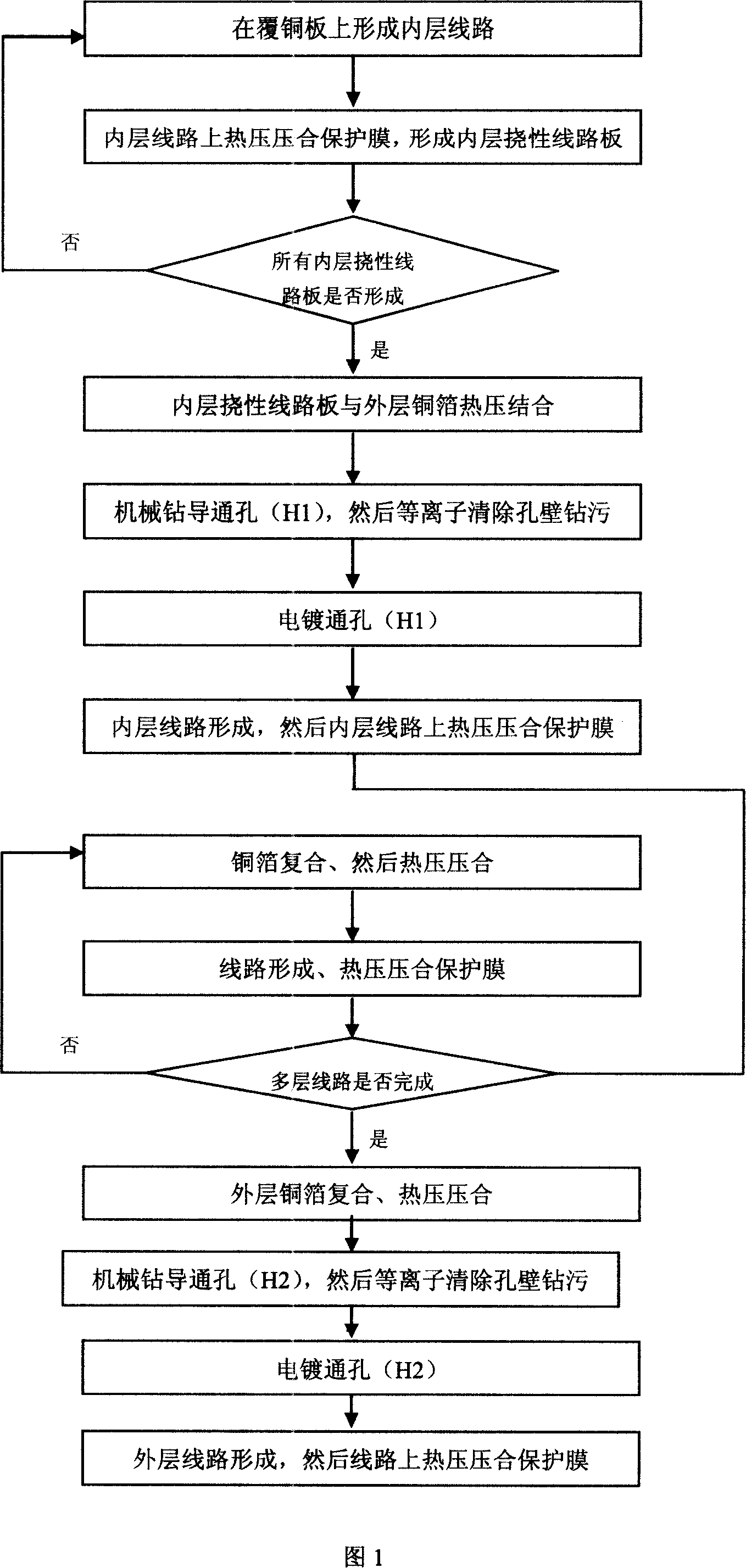
[0024] Described in the detailed description is a flexible four-layer circuit board and its manufacturing method.

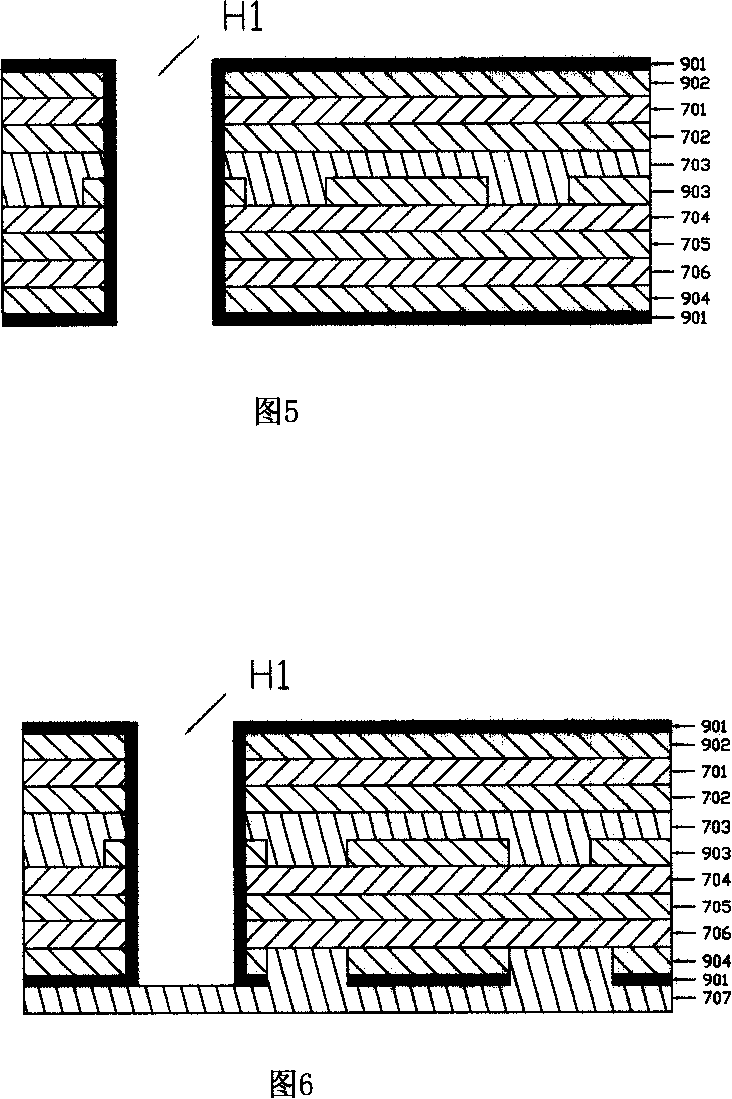
[0025] The four-layer flexible multilayer circuit board includes a blind hole H1 connecting the three-layer circuit board and a through hole H2 penetrating the four-layer circuit board. The blind hole H1 and the through hole H2 are marked in Fig. 2 to Fig. 9 . The position of the blind hole H1 is determined according to the wiring requirements of the circuit board in practical applications.

[0026] The method for manufacturing the four-layer flexible multilayer circuit board will be described below.

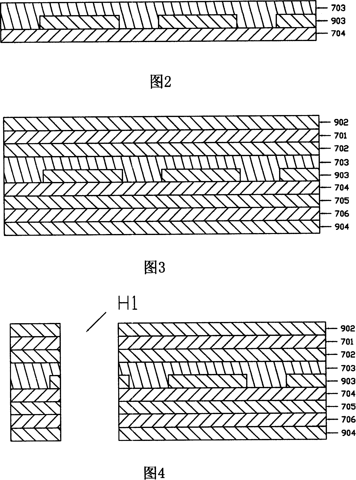
[0027] Referring to FIG. 2 to FIG. 10 , firstly, in FIG. 2 , the steps of forming and laminating a protective film for an inner layer circuit are laminated with protective layers 703 and 704 on both sides of copper foil 903 . In Fig. 3, one prepreg is pasted on both sides of the protective film 703, 704 and the substrate 702, 704 (polyimide resin), and two prepreg...


PUM


Abstract

The invention discloses a multi-layer flexible wiring board and manufacturing method therefor. The multi-layer flexible wiring board has at least three layers, which is characterized in that the wiring board comprises blind holes which only penetrate part of layer wiring boards and through holes penetrate all layer wiring boards. The invention adopts blind holes and through holes to connect layer by layer of the wiring board, the blind holes only need to drill through part of wiring boards, thereby wiring boards which are not be drilled through increase usable area, not all holes adopt perforated method, aligned deviation ratio between each layer is reduced, the number of joints is reduced, thereby reducing derivtion probability of short curcuits and open curcuits.

Description

technical field [0001] The invention relates to a flexible printed circuit board, more specifically to a flexible multilayer circuit board and a manufacturing method thereof. Background technique [0002] Flexible printed circuit boards are developing toward high density, and the structure of multilayer circuit boards is the most commonly used type. As shown in FIG. 9 , it is composed of a plurality of insulating layers 700-710 stacked up and down in sequence and inner layer copper foils 900-905 located therebetween. Each layer of material is combined with semi-cured glue as an adhesive and pressed together, and the layers of copper foil are not connected. Therefore, in order to connect some or specific parts of the lines of each layer, it is necessary to form the through hole H2 by drilling, and then go through the step of electroplating the through hole to make the inner wall surface of the through hole H2 and the surface of the flexible multilayer circuit board An elect...

Claims


Application Information

Patent Timeline
IPC IPC(8): H05K1/00H05K3/46
Inventor 代新
Owner 深圳市合力泰光电有限公司
Why Eureka
Try Eureka