Electro-optic device and electronic device

An electro-optic device and electro-optic technology, applied in optics, nonlinear optics, instruments, etc., can solve problems such as unclear tail, inability to obtain smooth dynamic images, image residual images, etc., to weaken the transverse electric field, reduce residual images and drag Effect of tailing phenomenon and suppression of decrease in aperture ratio

Inactive Publication Date: 2008-04-16
SEIKO EPSON CORP
View PDF1 Cites 6 Cited by
  • Summary
  • Abstract
  • Description
  • Claims
  • Application Information

AI Technical Summary

Problems solved by technology

[0006] As far as this electro-optical device is concerned, when a dynamic image is displayed, the residual image and the trailing phenomenon of the image will be generated due to the influence of the transverse electric field (when the dynamic image is displayed, the moving object leaves a residual image, which looks A phenomenon in which a smooth moving image cannot be obtained because it is unclear)

Method used


Image

  • Electro-optic device and electronic device
  • Electro-optic device and electronic device
  • Electro-optic device and electronic device

Examples


no. 1 Embodiment approach

[0059]

[0060]

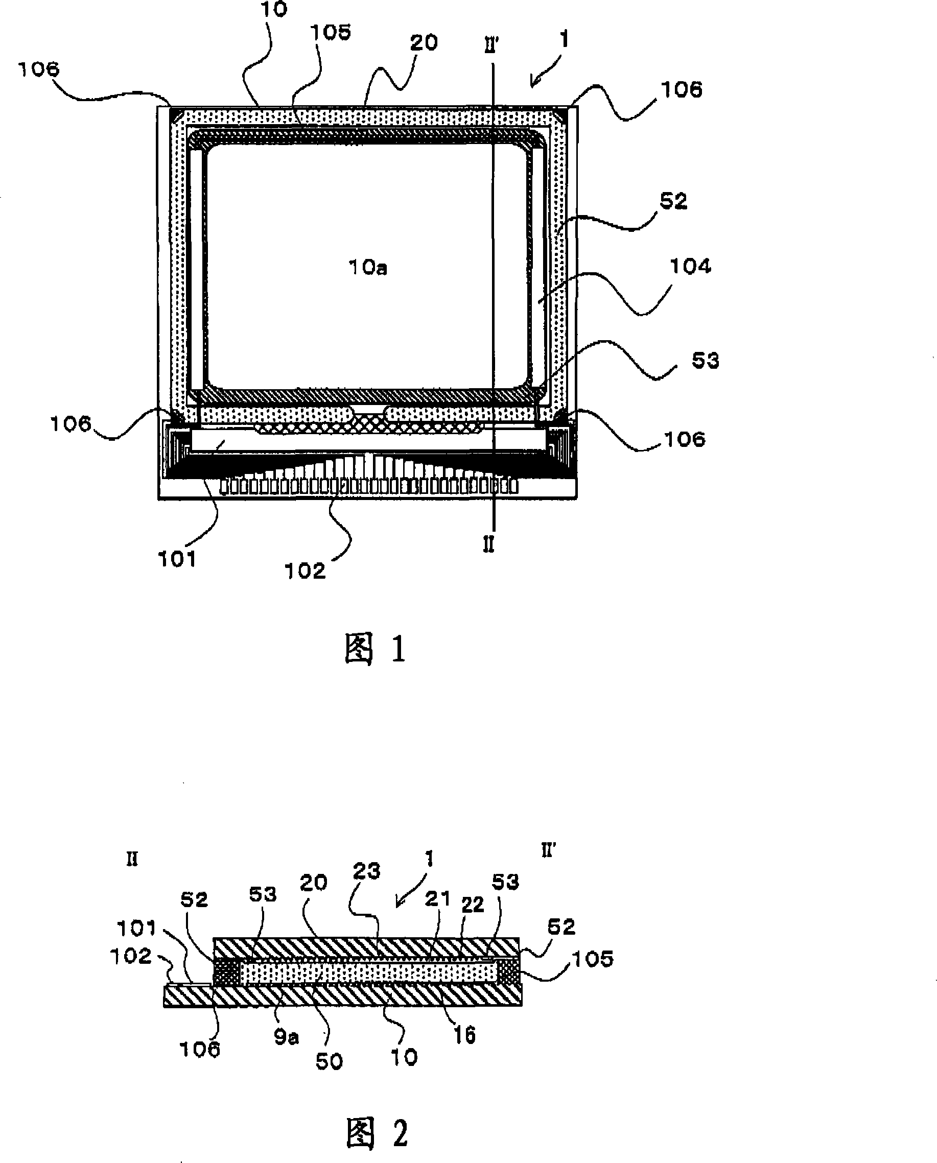
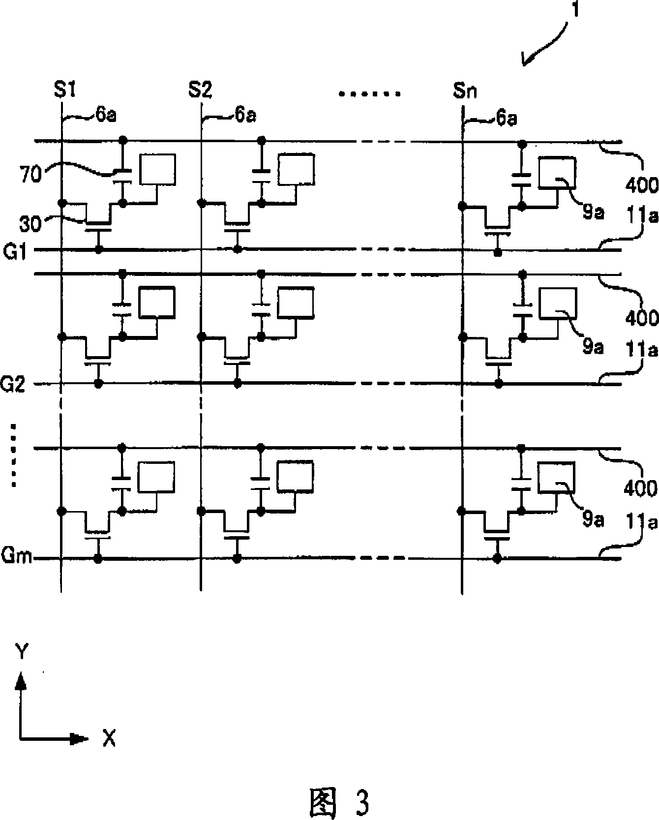
[0061] First, the electro-optical device according to the present embodiment will be described with reference to FIGS. 1 and 2 . FIG. 1 is a top view of an electro-optic device with a TFT array substrate and various structural elements formed thereon seen from the opposite substrate side, and FIG. 2 is a cross-sectional view along II-II' of FIG. 1 . In the present embodiment, as an example of an electro-optical device, a liquid crystal device of a TFT active matrix driving method with a built-in driver circuit will be taken as an example.

[0062] In FIGS. 1 and 2 , in the liquid crystal device 1 , the TFT array substrate 10 and the counter substrate 20 are arranged to face each other. A liquid crystal layer 50 is sealed between the TFT array substrate 10 and the opposite substrate 20, and the TFT array substrate 10 and the opposite substrate 20 are bonded to each other by a sealing material 52 disposed in a sealing area, which is located as a location wh...

no. 2 Embodiment approach

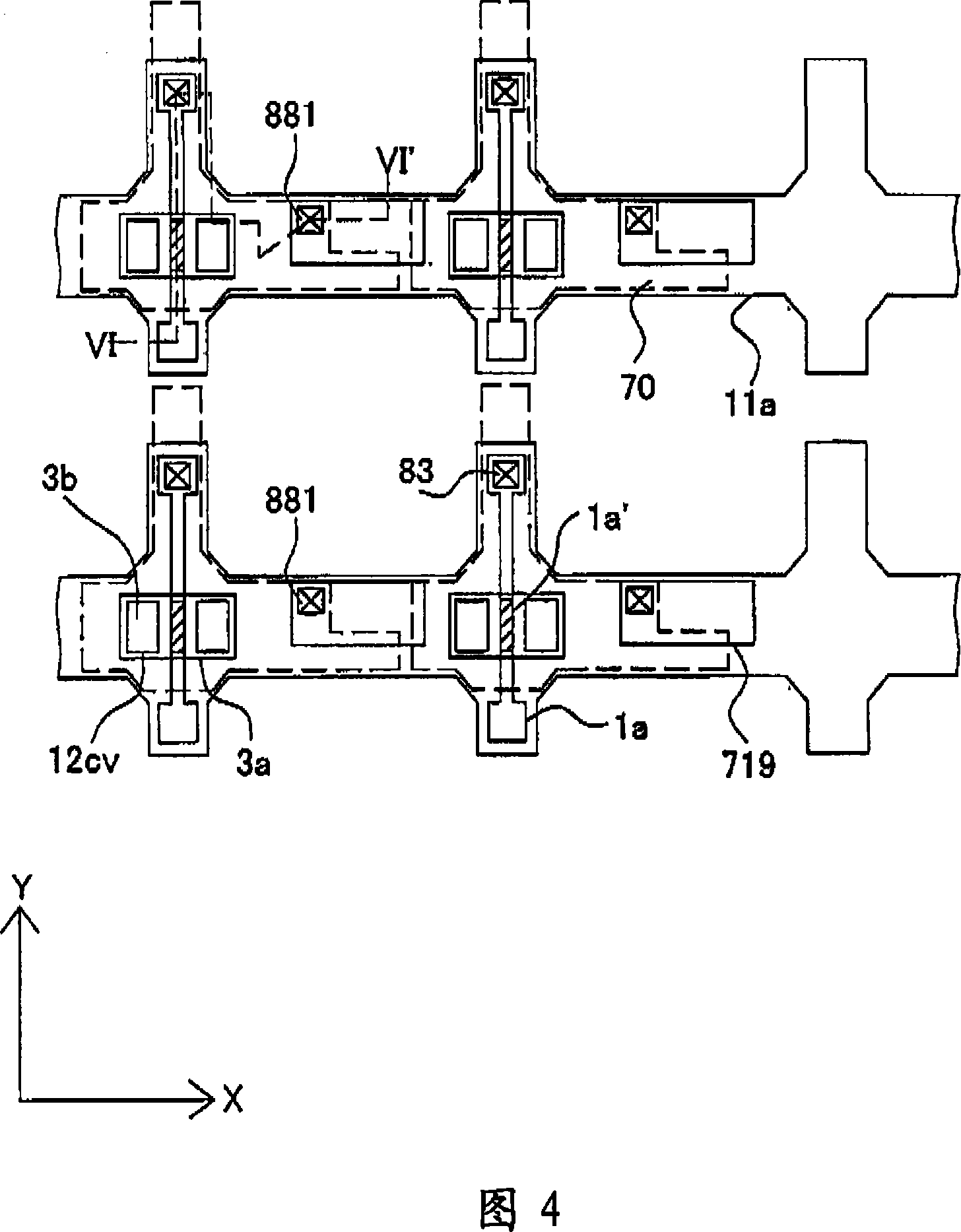
[0121] Next, the electro-optical device according to this embodiment will be described with reference to FIGS. 9 to 12 . In the following, the same parts as those of the electro-optical device according to the first embodiment will be omitted from illustration, and detailed descriptions will be omitted. In addition, the electro-optical device according to this embodiment has the same structure as the cross-sectional structure shown in FIG. In the driving method such as driving, in the vertical line inversion driving, images with different polarities are supplied to each of the data lines 6a adjacent to each other among the data lines 6a which are examples of the "image signal lines" in the second invention of the present invention The signals, that is, image signals having different potentials and polarities with respect to the counter electrode 21 are supplied, and in this dot inversion drive, image signals having different polarities are supplied to adjacent pixels.

[0122...


PUM


Abstract

The present invention provides a photoelectric device and an electronic equipment, which are used for reducing the bad states of residual image and lag phenomenon and the like which are generated when the dynamic image is displayed. The external shape of the pixel electrode (9a1-1) is approximately rectangular, a first edge part (29a1) facing to the pixel electrode (9a1-1) in the four edge parts extends along the X direction of the accompanying diagram and a dent (501) is arranged at one part of the edge part. The external shape of the pixel electrode (9a2-1) is same to the pixel electrode (9a1-1) and is approximate rectangular, a second edge part (29a2) facing to the pixel electrode (9a1-1) in the four edge parts extends along the X direction of the accompanying diagram and a convex part (502) is arranged at one part of the edge part. The convex part (502) and the region (R) restricted by the dent (501) coincidently extend from the second edge part (29a2) to the first edge part (29a1).

Description

technical field [0001] The present invention relates to the technical field of electro-optical devices such as liquid crystal devices and electronic equipment including such electro-optical devices. Background technique [0002] In a liquid crystal device as an example of such an electro-optic device, by applying a predetermined voltage between a pixel electrode and a counter electrode provided on a pair of substrates holding liquid crystals, the alignment state of liquid crystal molecules interposed between these electrodes is controlled, Instead the image is displayed. [0003] In such an electro-optical device, there sometimes arises a technical problem that the alignment of liquid crystal molecules is poor due to the following transverse electric field (that is, an electric field parallel to the substrate surface or an oblique electric field including a component parallel to the substrate surface) Therefore, the transverse electric field is generated between the pixel e...

Claims


Application Information

Patent Timeline
Patent Type & Authority Applications(China)
IPC IPC(8): G02F1/1343G02F1/1362G02F1/133
Inventor 尾野雄大山田周平
Owner SEIKO EPSON CORP
Why Eureka
Try Eureka