Semiconductor package structure and manufacture method thereof

A packaging structure and manufacturing method technology, which is applied in semiconductor/solid-state device manufacturing, semiconductor devices, semiconductor/solid-state device components, etc., can solve problems such as difficult, difficult to detect packages, production costs and time waste

Inactive Publication Date: 2008-04-23
卓恩民
View PDF0 Cites 6 Cited by
  • Summary
  • Abstract
  • Description
  • Claims
  • Application Information

AI Technical Summary

Problems solved by technology

[0004] However, in the above packaging structure, after the chip 200 and the passive component 300 are packaged, the electrical test is performed. The package body 400) must be scrapped, resulting in waste of production cost and time
On the other hand, when inspecting packages with poor electrical properties, because of the sealed structure, it is difficult to detect the cause of electrical failure inside the package, so it is difficult to improve the pass rate with the original structure

Method used


Image

  • Semiconductor package structure and manufacture method thereof
  • Semiconductor package structure and manufacture method thereof
  • Semiconductor package structure and manufacture method thereof

Examples


Embodiment Construction

[0035] The detailed description is as follows, and the preferred embodiment is only for illustration and not intended to limit the present invention.

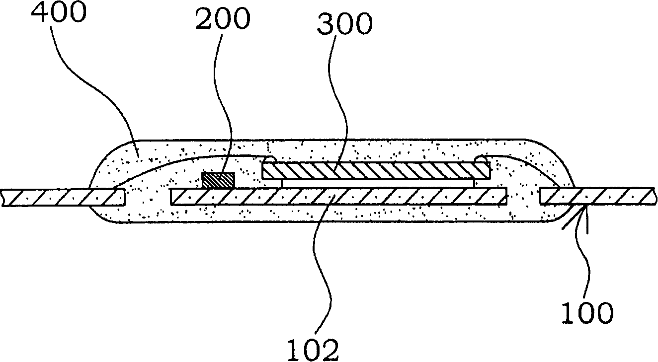
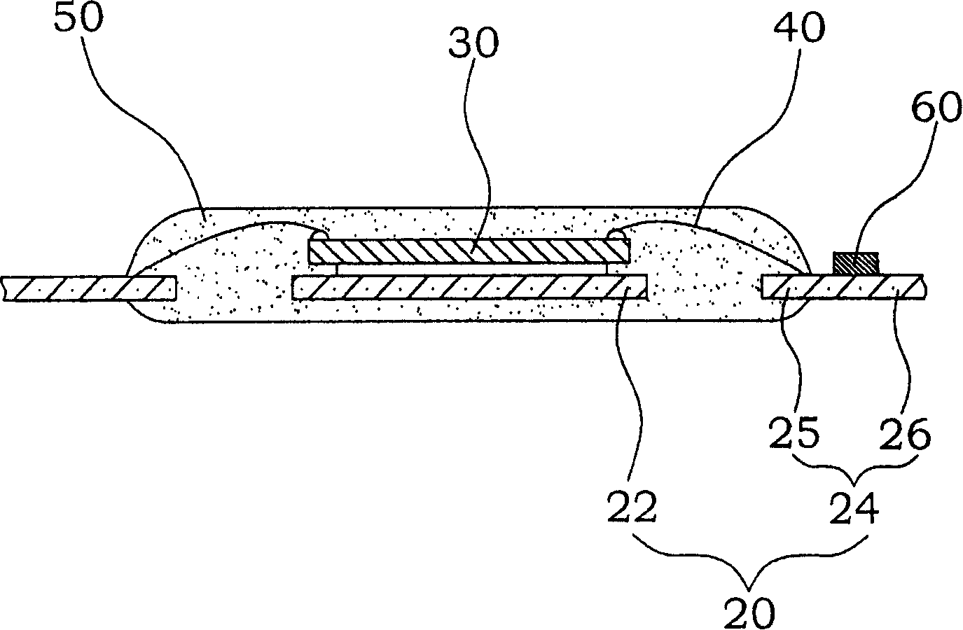
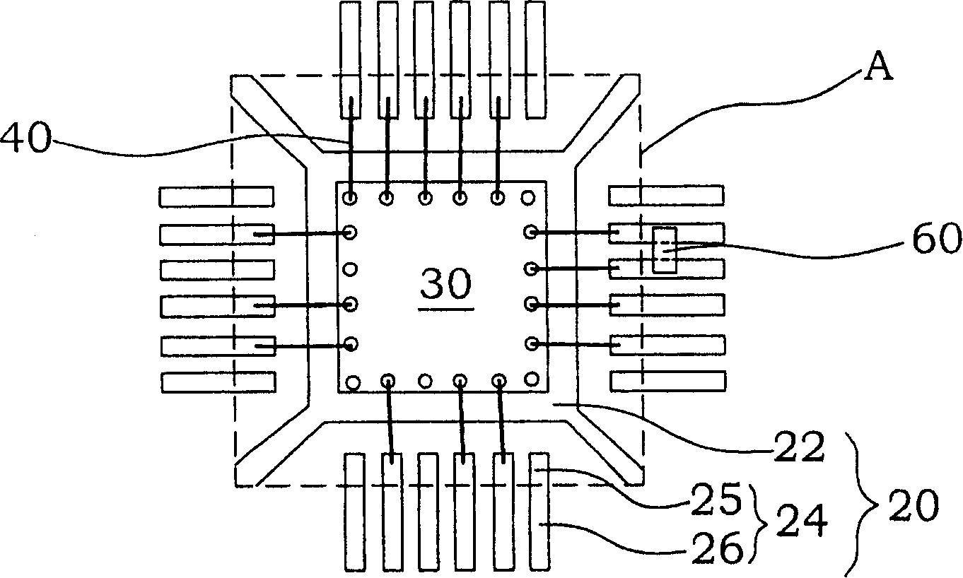
[0036] figure 2 Shown is a cross-sectional view of a semiconductor package structure according to an embodiment of the present invention. In this embodiment, the semiconductor packaging structure includes a lead frame 20 , a chip 30 , a molding compound 50 and a passive element 60 . like figure 2 As shown, the lead frame 20 contains a support member 22 and a plurality of pins 24, wherein any pin 24 contains an inner pin portion 25 and an outer pin portion 26; the chip 30 is in a suitable manner, such as a pasting method, It is arranged on the support member 22, and uses a conductive connecting element 40 to electrically connect the inner pin portion 25; a packaging compound 50, covering the chip 30, the conductive connecting element 40 and the inner pin portion 25 of the lead frame 20, on a In an embodiment, the material o...


PUM


Abstract

The semiconductor encapsulation structure comprises: a wire carrier, a chip, an encapsulation gel and a passive component located at the external pin area and the one of the support leg of the wire carrier; wherein, the passive3 component is exposed from the sealing gel; after the chip is encapsulated, the passive component is configured.

Description

technical field [0001] The invention relates to a semiconductor packaging technology, in particular to a semiconductor packaging structure with passive components and a manufacturing method thereof. Background technique [0002] With the advancement of semiconductor process technology and the increasing density of integrated circuits, there are more and more pins in the structure of components, and the requirements for speed are getting faster and faster, which makes the production of small, fast and high-density structure components Has become a trend. [0003] As the construction speed of electronic packages increases, noise from DC power lines and ground lines has gradually become a problem that cannot be ignored. Therefore, passive components, such as capacitance, are generally used to reduce power supply noise. figure 1 A cross-sectional view of a semiconductor package structure with passive components in the prior art is shown, which includes a lead frame 100 , a chi...

Claims


Application Information

Patent Timeline
Patent Type & Authority Applications(China)
IPC IPC(8): H01L25/00H01L25/16H01L23/31H01L23/488H01L23/495H01L21/56H01L21/60
CPCH01L2924/14H01L2924/01079H01L2224/48091H01L2224/49175H01L2924/30107H01L2224/48247H01L2224/73265H01L2924/181
Inventor 卓恩民
Owner 卓恩民
Why Eureka
Try Eureka