

Solid-state imaging device, imaging apparatus
A solid-state imaging device and pixel technology, applied in radiation control devices, electrical components, image communication, etc., can solve the problem of difficult to reduce pixel size, unfavorable high-speed drive, increase pixel circuit drive load, signal readout load of pixel circuit, etc. problem, to achieve the effect of simplifying wiring, improving area utilization efficiency, and effective pixel layout
Inactive Publication Date: 2010-11-10
SONY CORP
View PDF3 Cites 0 Cited by
- Summary
- Abstract
- Description
- Claims
- Application Information
AI Technical Summary
Problems solved by technology
However, CMOS imaging devices include many driver elements such as photodiodes, transfer transistors, reset transistors, amplification transistors, selection transistors, etc. within one pixel, and thus, it is difficult to reduce the size of the pixels
Also, since the number of pixels is increased, the driving load of the pixel circuit and the readout load of a signal from the pixel circuit are increased, which leads to a situation that is not conducive to high-speed driving
Method used
View moreImage
Smart ImageViewing Examples

Examples
no. 3 example
no. 4 example
no. 5 example
Login to View More PUM
 Abstract
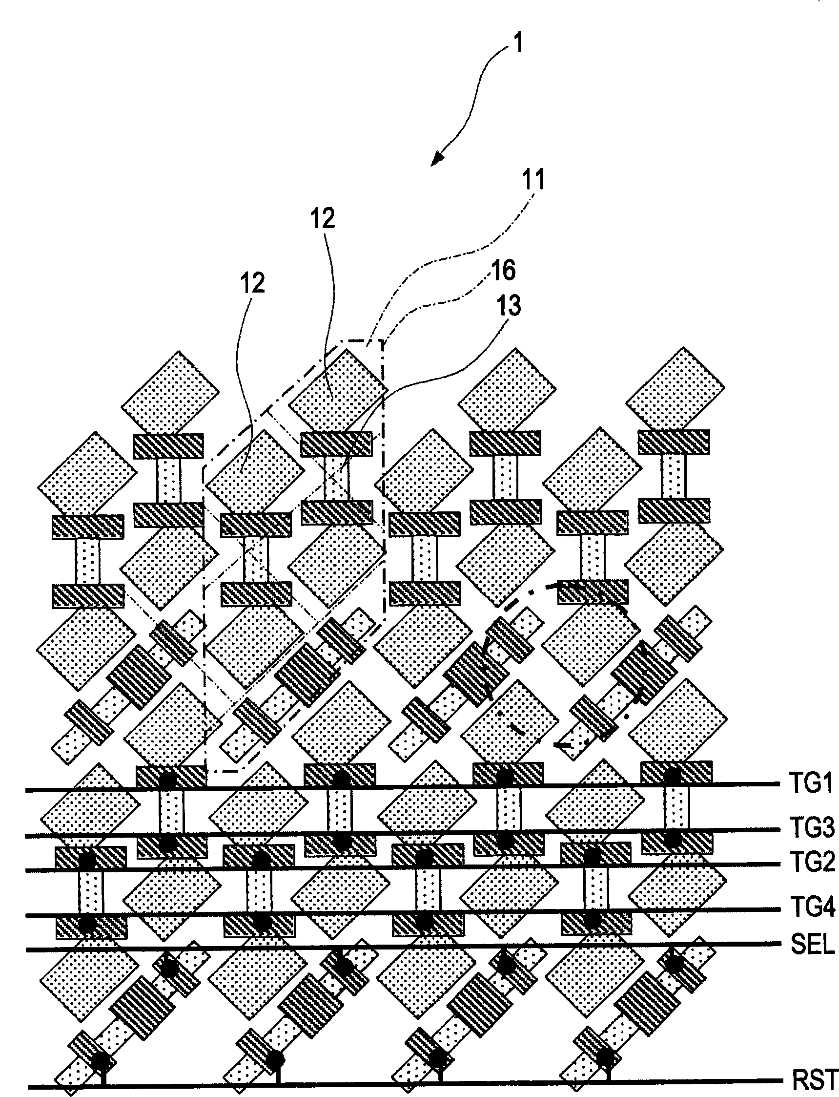
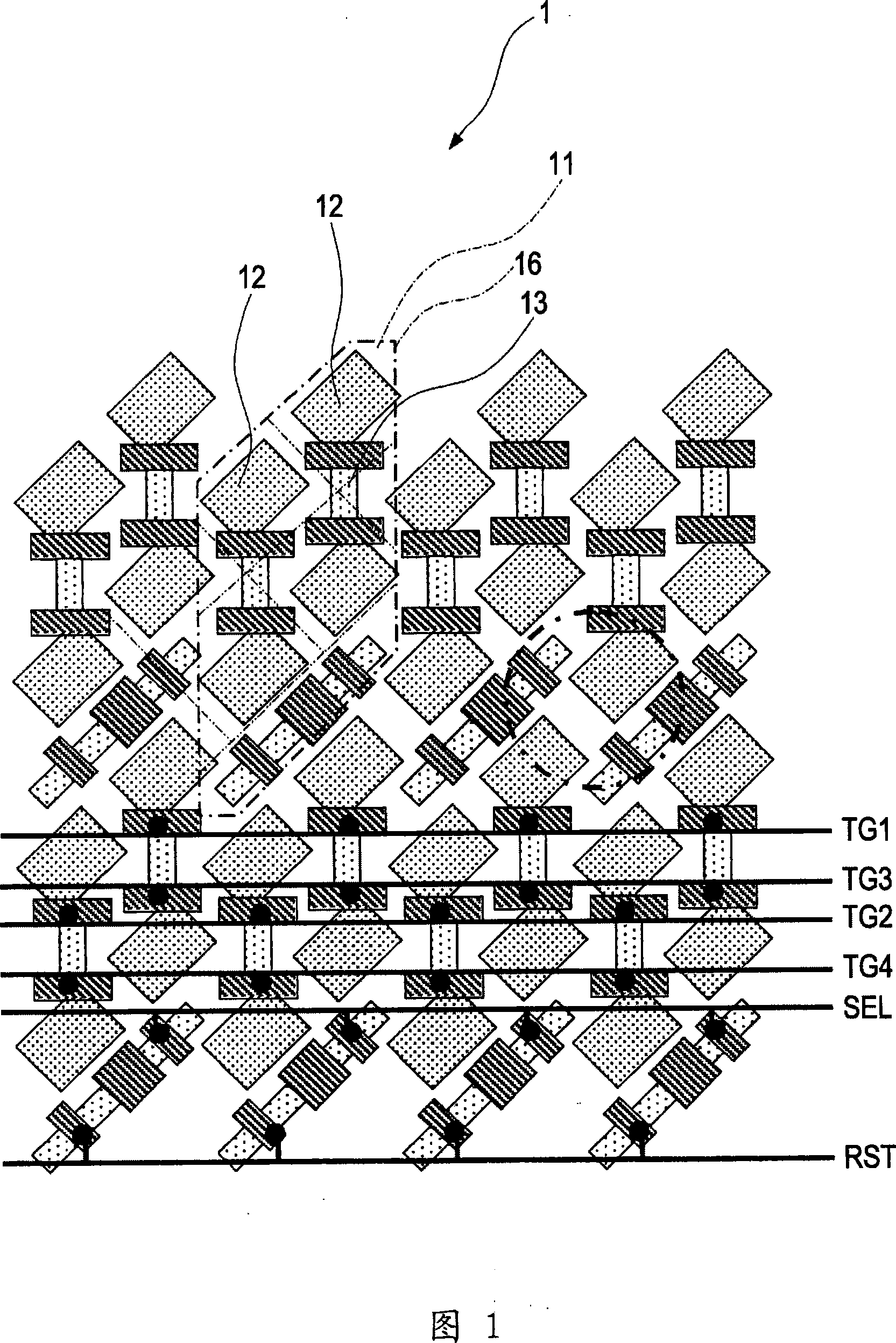
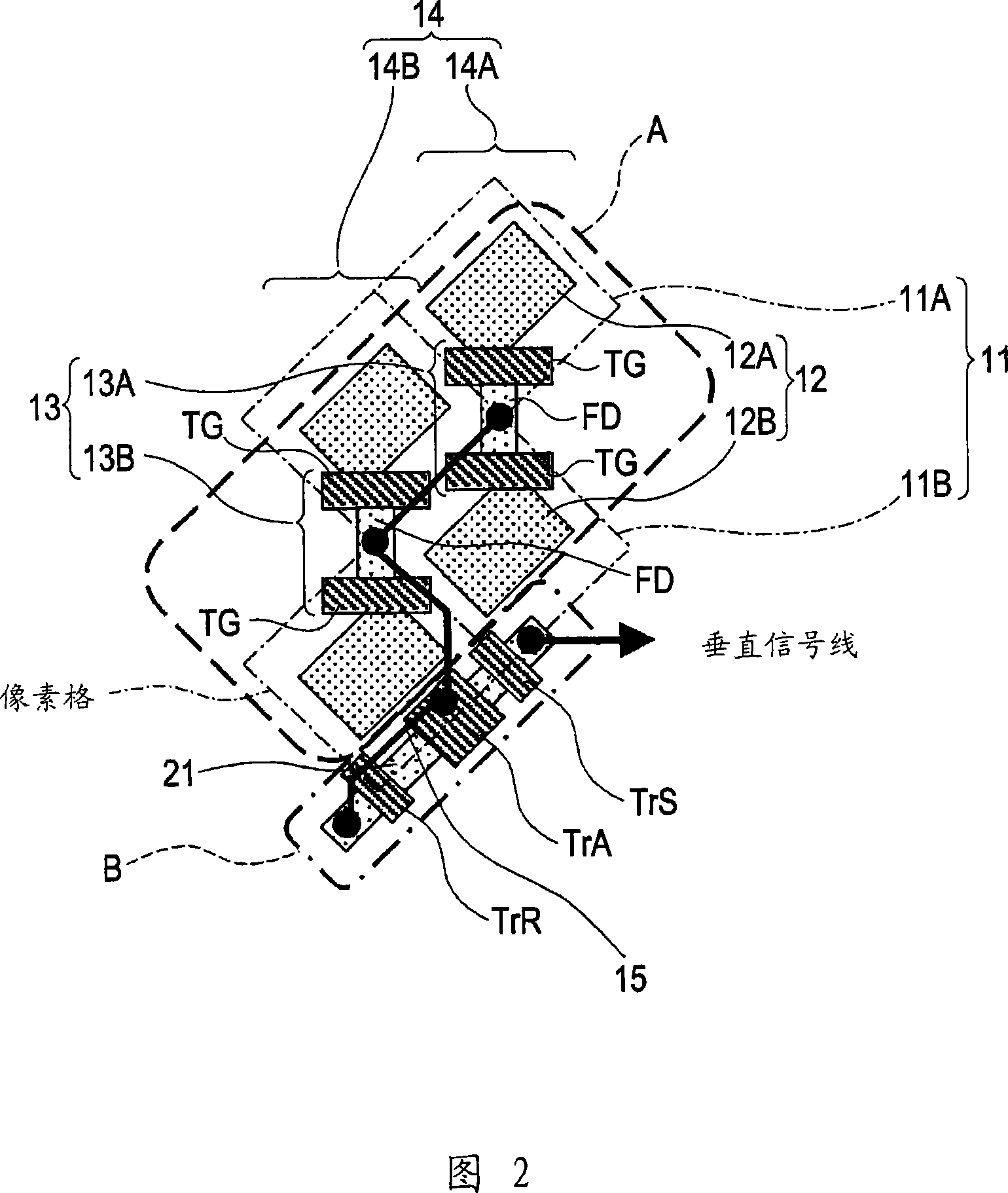
A solid-state imaging device includes: multiple pixels making up a slanted grid array inclined to a scanning direction, which include a photoelectric conversion unit configured to convert incident light quantity into an electric signal; and a charge-to-voltage conversion unit configured to convert signal charge read out from the photoelectric conversion unit disposed between two pixels adjacent to each other in the diagonal direction of the pixels of the multiple pixels into voltage; wherein the charge-to-voltage conversion unit is shared with the two pixels; and wherein a set of transistor group are disposed in a sharing block, which is configured of a pixel pair made up of the two pixels adjacent to each other in the diagonal direction, and a pixel pair adjacent to that pixel pair, including wiring to which the charge-to-voltage conversion unit of each pixel pair is connected.
Description
Solid-state imaging device and imaging device Cross References to Related Applications The present invention encompasses subject matter related to Japanese Patent Application JP2006-279733 filed with the Japan Patent Office on October 13, 2006, Japanese Patent Application JP2006-306278 filed with the Japan Patent Office on November 13, 2006, and Japanese Patent Application JP2006-306278 filed with the Japan Patent Office on March 2, 2007 Japanese Patent Application JP2007-052935 filed by the Japanese Patent Office, the entire contents of which are hereby incorporated by reference. technical field The present invention relates to a solid-state imaging device and an imaging device. And, the present invention also relates to an imaging device and a camera including an imaging device such as a CCD (Charge Coupled Device), a CMOS (Complementary Metal Oxide Semiconductor) sensor, or the like. Background technique Since digital cameras have been widely used in recent years, e...
Claims
Login to View More Application Information
Patent Timeline
 Patent Type & AuthorityPatents(China)
IPC IPC(8): H04N5/374H01L27/146H04N5/369H04N5/335
Inventor工藤义治
OwnerSONY CORP