
Power-on reset circuit

A technology for resetting circuits and power supply voltages, which can be used in data resetting devices, electrical components, electronic switches, etc., and can solve problems such as malfunctions

Inactive Publication Date: 2012-01-11
LAPIS SEMICON CO LTD
View PDF1 Cites 0 Cited by
  • Summary
  • Abstract
  • Description
  • Claims
  • Application Information

AI Technical Summary

Problems solved by technology

Therefore, a through current flows every time the power is turned on, which may cause malfunction due to deterioration over time.

Method used


Image

  • Power-on reset circuit
  • Power-on reset circuit
  • Power-on reset circuit

Examples


Embodiment 1

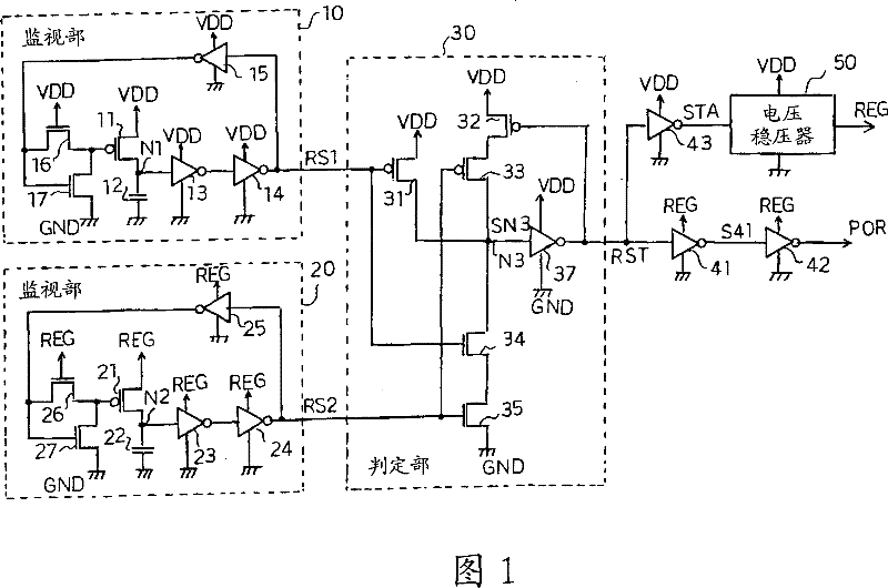
[0035] figure 1 It is a configuration diagram showing a power-on reset circuit according to Embodiment 1 of the present invention.

[0036] This power-on reset circuit supports two types of power supply voltages: a power supply voltage VDD supplied from the outside and a power supply voltage REG adjusted by an internal voltage regulator (where VDD>REG).

[0037] This power-on reset circuit includes: a monitoring unit 10 that monitors a rise in a power supply voltage VDD and outputs a reset signal RS1; and a monitor unit 20 that monitors a rise in a power supply voltage REG and outputs a reset signal RS2.

[0038] The monitoring unit 10 has a PMOS 11 connected between a power supply voltage VDD and a node N1, and a time constant circuit using a capacitor 12 connected between the node N1 and a ground potential GND. Inverters 13 , 14 , and 15 driven by power supply voltage VDD are vertically connected to node N1 , and a reset signal RS1 is output from the output side of the inver...

Embodiment 2

[0057] Figure 5 is a structural diagram showing a power-on reset circuit according to Embodiment 2 of the present invention, and figure 1 The same symbols are assigned to the elements in which the elements are the same.

[0058] The power-on reset current is provided with a judging section 30A with a slightly different structure instead of figure 1 The judging part 30 in. That is, in the determination unit 30A, an NMOS 36 is added between the node N3 and the ground potential GND to control its conduction state by the reset signal RST. Also, the size of NMOS 36 is set to be equal to or less than half the size of NMOS 34 and 35 . This is because NMOS 34 and 35 are connected in series in two stages, and NMOS 36 has a one-stage structure, so the current driving capability is simply doubled, and this NMOS 36 serves as an auxiliary function of NMOS 34 and 35 , so it does not require such a large current driving capability. other structures with figure 1 same.

[0059] In t...


PUM


Abstract

The invention provides an energizing reset circuit which prevents the perforation current in the energizing reset circuit corresponding to the two power voltages. A judging part (30) takes the reset signal (RS1) outputted from an inspection part (10) of an inspection outside power voltage (VDD) and the logical AND of a reset signal (RS2) outputted from an inspection part (20) of the inspection inside power voltage (REG), outputting the reset signal (RST). The judging part (30) is inserted PMOS (32) with PMOS (33) in series which is connected between the power voltage (VDD) and a node (N3). The conduction state is controlled by adopting the inspection signal (RS2) and the conduction state of the PMOS (32) is controlled by adopting the reset signal (RST). Therefore, even the inspection signal (RS2) is instable causing the simultaneous conduction of the PMOS (33) and the NMOS (35), the PMOS (32) can be stopped, without flowing the perforation current.

Description

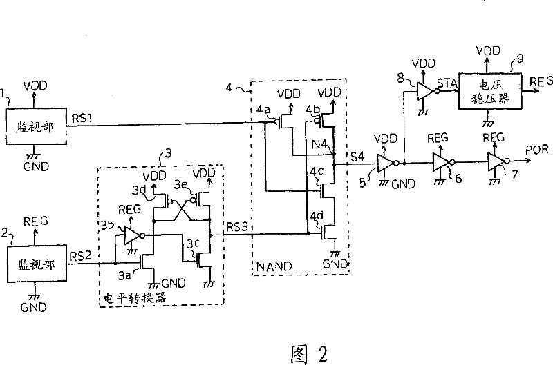
technical field [0001] The present invention relates to a power-on reset circuit for monitoring the rise of a power supply and putting an internal circuit in a reset state until the power rises to a predetermined level. Background technique [0002] figure 2 This is a configuration diagram of a conventional power-on reset circuit. [0003] This power-on reset circuit supports two types of power supply voltages: a power supply voltage VDD supplied from the outside and a power supply voltage REG regulated by an internal voltage regulator. [0004] This power-on reset circuit includes: a monitoring unit 1 that monitors a rise in a power supply voltage VDD and outputs a reset signal RS1; and a monitor unit 2 that monitors a rise in a power supply voltage REG and outputs a reset signal RS2. Both monitors 1 and 2 have the same configuration, and use a CR time constant circuit based on the capacitance C of the capacitor and the on-resistance R of the transistor to determine the v...

Claims


Application Information

Patent Timeline
Patent Type & Authority Patents(China)
IPC IPC(8): H03K17/22H03K17/687
CPCG06F1/24H03K17/22
Inventor 杉尾贤一郎
Owner LAPIS SEMICON CO LTD
Learn More