An inverter motherboard etching equipment

An etching equipment and an inverter technology, applied in the field of inverter motherboard etching equipment, can solve problems such as difficult to avoid side erosion phenomenon, and achieve the effect of avoiding side erosion phenomenon

Active Publication Date: 2021-06-01
NANJING VOCATIONAL UNIV OF IND TECH
View PDF3 Cites 0 Cited by
  • Summary
  • Abstract
  • Description
  • Claims
  • Application Information

AI Technical Summary

Problems solved by technology

[0003] Therefore, it is necessary to reduce the occurrence of side erosion, and the current commonly used etching methods, whether it is intrusion etching or spray etching, are difficult to avoid the occurrence of side erosion

Method used


Image

  • An inverter motherboard etching equipment
  • An inverter motherboard etching equipment
  • An inverter motherboard etching equipment

Examples


Embodiment Construction

[0028] In order to make the technical means, creative features, goals and effects achieved by the present invention easy to understand, the present invention will be further described below in conjunction with specific embodiments.

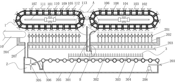
[0029] like Figure 1 to Figure 7 As shown, an inverter main board etching equipment includes a transfer mechanism 1, an etching mechanism 2 and a discharge assembly 3, the etching mechanism 2 is located directly below the transfer mechanism 1, the discharge assembly 3 etches the middle of the mechanism 2, and Mechanism 1 is provided with two opposite groups, the transfer mechanism 1 on the left rotates counterclockwise, and the transfer mechanism 1 on the right rotates clockwise;

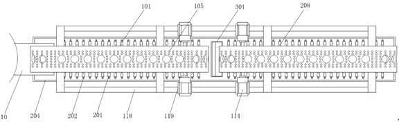
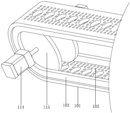
[0030] The transfer mechanism 1 includes an outer crawler 101 and an inner crawler 102 rotatably connected between two outer plates 104, the inner crawler 102 is located inside the outer crawler 101, and the outer crawler 101 is divided into an outer cavity 112 and an ...


PUM


Abstract

The invention discloses an inverter main board etching device, which relates to the field of equipment main board etching processing, and includes a transfer mechanism, an etching mechanism and a discharge assembly, the etching mechanism is located directly below the transfer mechanism, the middle part of the discharge assembly etching mechanism, and the transfer The mechanism is equipped with two sets of opposite groups. By setting the spray from bottom to top, the etching solution is sprayed to the lower surface of the PCB board for etching. The etching solution will directly drip down from the lower surface of the PCB board and will not flow through the side of the PCB board; And the top of the PCB board will continuously blow air downwards, and the PCB board itself will block the airflow directly above it, so it will not hinder the spraying of the etching solution directly below the PCB board, while the airflow next to the PCB board will blow away and spray to the PCB The etchant on the side of the board prevents the side of the PCB from coming into contact with the etchant and avoids side erosion.

Description

technical field [0001] The invention relates to the field of equipment main board etching processing, in particular to an inverter main board etching equipment. Background technique [0002] The motherboards of various electrical equipment are composed of various basic components on the PCB, and most of the circuits in the PCB are etched, such as the inverter motherboard. Nowadays, with the development of electronic products, there are higher requirements for the accuracy of PCB boards. [0003] Therefore, it is necessary to reduce the occurrence of side erosion, and the current commonly used etching methods, whether it is intrusion etching or spray etching, cannot avoid the occurrence of side erosion. Among them, spray etching can greatly improve the side erosion phenomenon. [0004] There are two main reasons for the side erosion caused by spray etching. One is that when spraying, the etching solution will also be sprayed to the side of the PCB board. The second is that...

Claims


Application Information

Patent Timeline
Patent Type & Authority Patents(China)
IPC IPC(8): H05K3/06
CPCH05K3/06H05K3/068
Inventor 何智勇
Owner NANJING VOCATIONAL UNIV OF IND TECH
Why Eureka
Try Eureka