Image display system comprising low temperature poly silicon thin film transistor and its manufacture method

An image display system and thin-film transistor technology, which is applied in transistors, semiconductor/solid-state device manufacturing, electric solid-state devices, etc., can solve problems such as oxide layer charge diffusion, N-type thin-film transistor components cannot be turned off normally, and critical voltage shift

Inactive Publication Date: 2008-06-04
TPO DISPLAY
View PDF0 Cites 6 Cited by
  • Summary
  • Abstract
  • Description
  • Claims
  • Application Information

AI Technical Summary

Problems solved by technology

However, the P-type thin film transistor device suffers from the so-called "threshold voltage shift" problem (as shown in Figure 3B) after the device undergoes a high-pressure annealing process.
At the same time, the N-type TFT element cannot be turned off normally, as shown in Figure 3A
As a result, the circuitry of the panel may not operate
In addition, the residual oxide charge that may be caused by the high pressure annealing process will diffuse to the active area of ​​the device

Method used


Image

  • Image display system comprising low temperature poly silicon thin film transistor and its manufacture method
  • Image display system comprising low temperature poly silicon thin film transistor and its manufacture method
  • Image display system comprising low temperature poly silicon thin film transistor and its manufacture method

Examples


no. 1 example

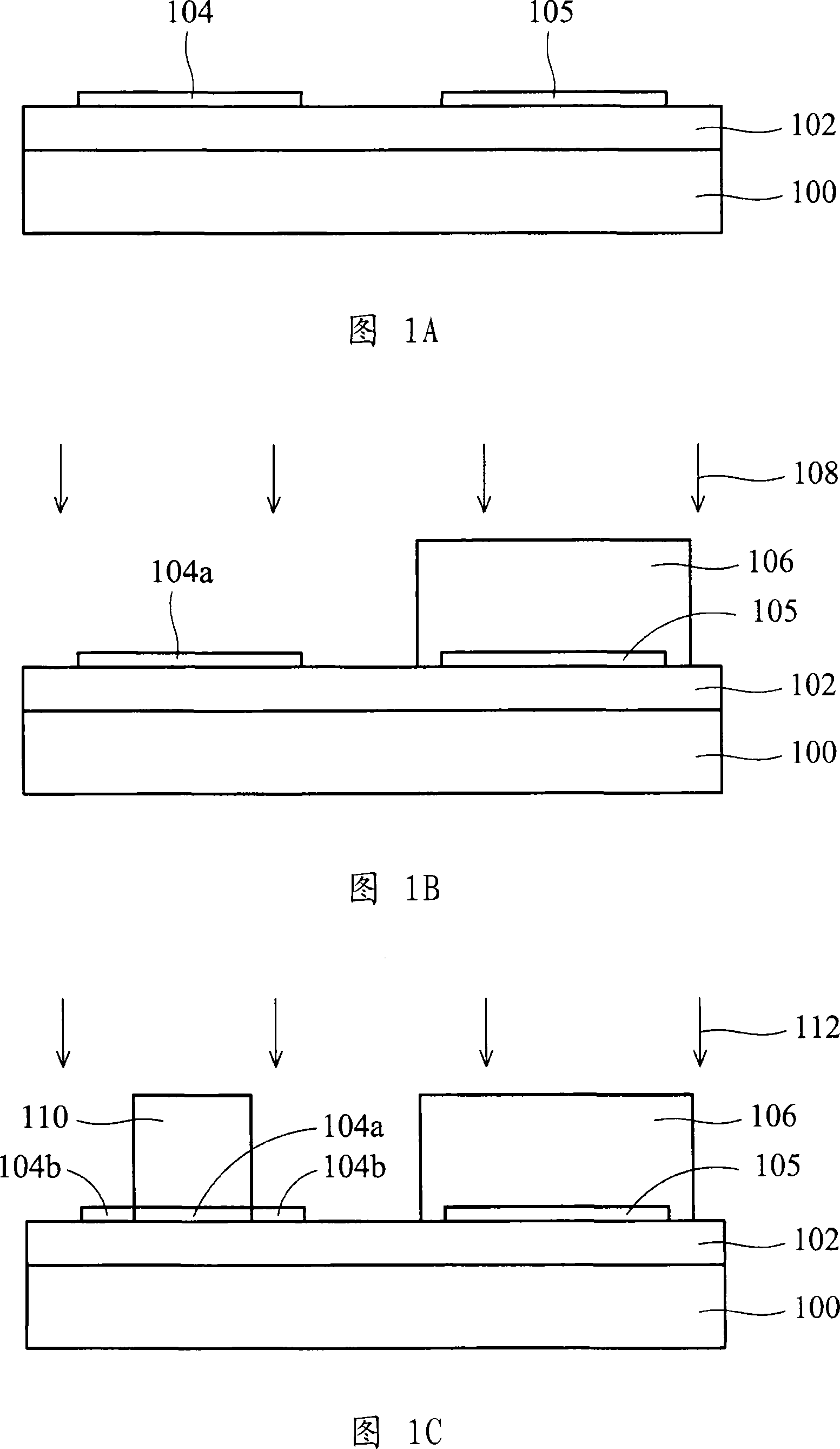
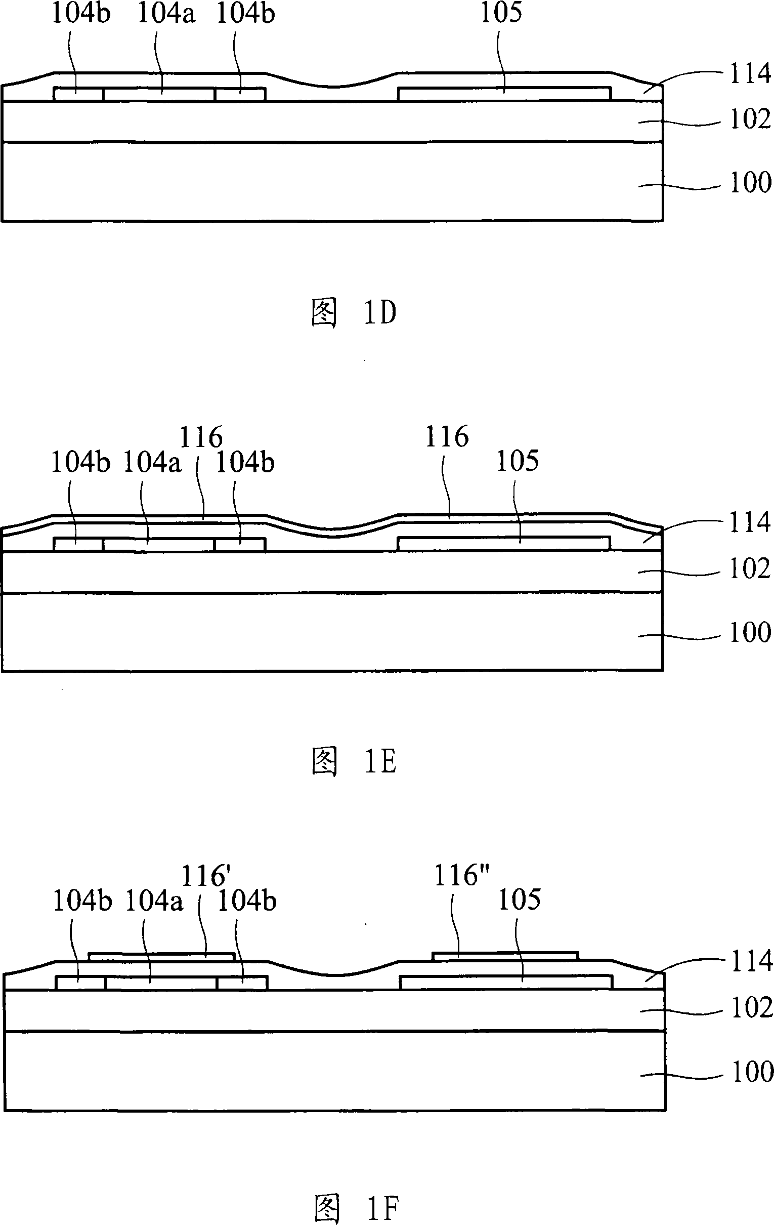
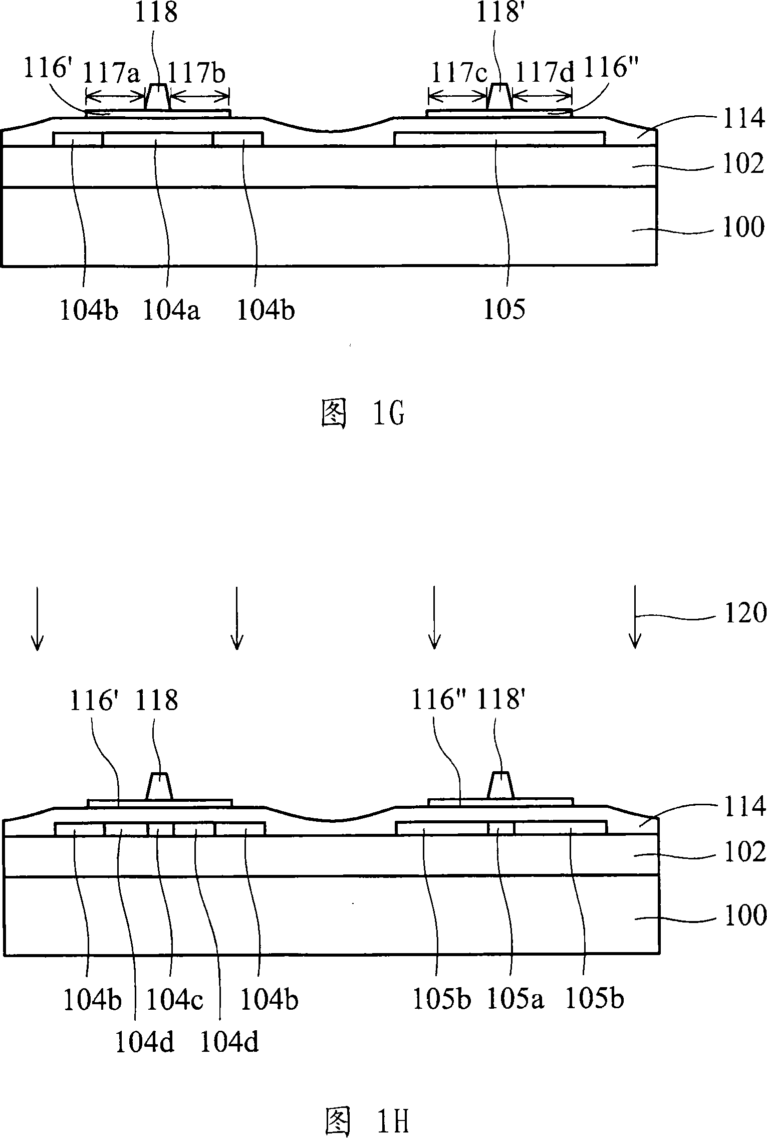
[0018] As shown in FIG. 1L , in the low temperature polysilicon thin film transistor liquid crystal display of the first embodiment, a buffer layer 102 is located on the substrate 100 . An active layer is located on the buffer layer 102, and at least includes a first active layer or a second active layer or both; the first active layer includes a channel region 104c, a lightly doped source / drain 104d, a source / drain electrode 104b; the second active layer includes a channel region 105a and a source / drain electrode 105c. The gate insulating layer 114 is located on the active layer and the buffer layer 102 . A dielectric layer is located on the gate insulating layer 114, and at least includes a first dielectric layer 116' or a second dielectric layer 116" or both. A first gate electrode 118 and a second gate The electrodes 118' are located on the first dielectric layer 116' or the second dielectric layer 116", respectively. The interlayer dielectric layer 126 is located on th...

no. 2 example

[0031] As shown in FIG. 2F , in the low temperature polysilicon thin film transistor liquid crystal display of the first embodiment, a buffer layer 202 is located on the substrate 200 . An active layer is located on the buffer layer 202, and at least includes a first active layer or a second active layer or both; the first active layer includes a channel region, lightly doped source / drain 204d, source / drain The drain electrode 204a; the second active layer includes a channel region 205b and a source / drain electrode 205c. The gate insulating layer 214 is located on the patterned active layer and the buffer layer 202 . A patterned dielectric layer is located on the gate insulating layer 214, and at least includes a first dielectric layer 216' or a second dielectric layer 216" or both. A first gate electrode 218 and a second The gate electrode 218' is located on the first dielectric layer 216' or the second dielectric layer 216", respectively. A first patterned protective layer...


PUM

PropertyMeasurementUnit
lengthaaaaaaaaaa
lengthaaaaaaaaaa
lengthaaaaaaaaaa

Abstract

The invention discloses an LTPS TFT-LCD comprising a plurality of NMOS elements and PMOS elements on a substrate. Each element comprises a SiNx layer underlying or capping a gate electrode. The SiNx layer features an appropriate length extending from the bottom edge of the gate electrode. The SiNx layer can be replaced with a SiOxNy layer.

Description

technical field [0001] The present invention relates to an image display system and its manufacturing method, and in particular to a low-temperature polysilicon thin film transistor liquid crystal display and its manufacturing method. Background technique [0002] In the conventional low-temperature polysilicon thin film transistor liquid crystal display process, a high pressure anneal process is generally performed on the switching element to improve the uniformity of the element characteristics. However, the current P-type thin film transistor device suffers from a so-called "threshold voltage shift" problem (as shown in FIG. 3B ) after the device undergoes a high pressure annealing process. At the same time, the N-type TFT device cannot be turned off normally, as shown in FIG. 3A . As a result, the circuits of the panel may not operate. In addition, the residual oxide charge that may be caused by the high pressure annealing process will diffuse to the active area of ​​t...

Claims


Application Information

Patent Timeline
Patent Type & Authority Applications(China)
IPC IPC(8): H01L29/786H01L29/423H01L27/12H01L21/336H01L21/28H01L21/84G02F1/1362
CPCH01L27/1214H01L29/4908H01L29/42384H01L27/12H01L27/127H01L27/1296
Inventor 曾章和王士宾刘俊彦许国斌
Owner TPO DISPLAY
Why Eureka
Try Eureka