LDMOS transistor

A transistor and seed crystal technology, applied in the field of LDMOS transistors, can solve problems such as reducing the life of LDMOS transistors, and achieve the effect of weakening Idq degradation and improving linear efficiency

Active Publication Date: 2008-07-09
AMPLEON NETHERLANDS
View PDF1 Cites 29 Cited by
  • Summary
  • Abstract
  • Description
  • Claims
  • Application Information

AI Technical Summary

Problems solved by technology

Accelerated I dq Degradation reduces the lifetime of LDMOS transistors

Method used


Image

  • LDMOS transistor
  • LDMOS transistor
  • LDMOS transistor

Examples


Embodiment Construction

[0022] The figures are not drawn to scale. In general, like components are designated with like reference numerals in these figures.

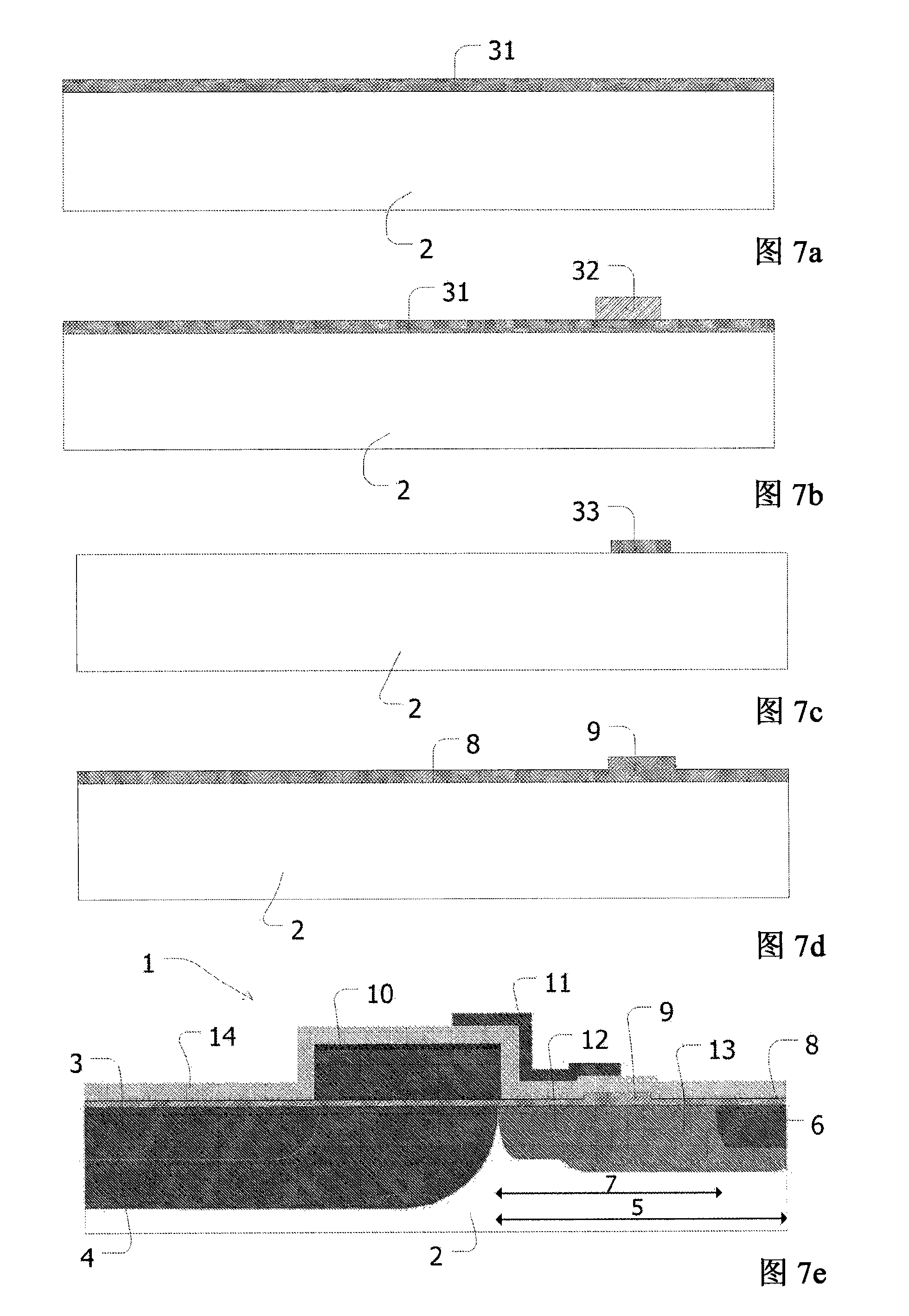
[0023] FIG. 1 shows a cross-sectional view of a conventional LDMOS transistor 99 according to the prior art. The LDMOS transistor 99 comprises a substrate 2 of semiconductor material, here p-type silicon. The LDMOS transistor 99 further comprises a silicided polysilicon gate electrode 10 extending through the p-type channel region 4 , and the n-type source region 3 and n-type drain region 5 , which are connected to each other through the p-type channel region 4 . Channel region 4 , source region 3 and drain region 5 are fabricated within substrate 2 . In this example, channel 4 is a laterally diffused p-type region. The gate electrode 10 and the substrate 2 are separated by a gate oxide layer 18, wherein the gate oxide layer 18 comprises thermally grown silicon dioxide, for example.

[0024] The drain region 5 includes an n-type drain epita...


PUM


Abstract

The LDMOS transistor (1) of the invention comprises a source region (3), a channel region (4), a drain extension region (7) and a gate electrode (10). The LDMOS transistor (1) further comprises a first gate oxide layer (8) and a second gate oxide layer (9), which is thicker than the first gate oxide layer (8). The first gate oxide layer (8) at least extends over a first portion of the channel region (4), which is adjacent to the source region (3). The second gate oxide layer (9) extends over a region where a local maximum (A, B) of the electric field (E) generates hot carriers thereby reducing the impact of the hot carriers and reducing the Idq-degradation. In another embodiment the second gate oxide layer (9) extends over a second portion of the channel region (4), which mutually connects the drain extension region (7) and the first portion of the channel region (4), thereby improving the linear efficiency of the LDMOS transistor (1).

Description

technical field [0001] The present invention relates to LDMOS transistors. Background technique [0002] RF power amplifiers are key components in base stations for personal communication systems (GSM, EDGE, W-CDMA). For these power amplifiers, RF laterally diffused metal-oxide-semiconductor (commonly abbreviated as LDMOS) transistors are becoming a preferred technology choice due to their outstanding high power handling, gain and linearity. The performance of LDMOS transistors, which are shrinking in size, is undergoing continuous improvement in order to meet the requirements imposed by new communication standards. [0003] An LDMOS transistor is disclosed in WO2005 / 022645, which is arranged on a semiconductor substrate and which comprises a source region and a drain region interconnected by a channel region, and a gate electrode. The drain region includes a drain contact region and a drain epitaxial region extending from the drain contact region to the channel region in...

Claims


Application Information

Patent Timeline
Patent Type & Authority Applications(China)
IPC IPC(8): H01L29/78H01L29/40H01L29/423H01L23/31H01L21/336H01L29/08
CPCH01L29/66659H01L29/0847H01L29/42368H01L29/402H01L29/7835H01L29/66681H01L29/7816
Inventor 弗雷尔克·范瑞哲斯蒂芬·J·C·H·特厄乌文彼得拉·C·A·哈梅斯
Owner AMPLEON NETHERLANDS
Why Eureka
Try Eureka