Blanking type encapsulation constitution without external pin and manufacturing method thereof

A manufacturing method and punching technology, used in semiconductor/solid-state device manufacturing, electrical components, electrical solid-state devices, etc., can solve the problems of pin cut surface burrs, increase the cut surface area, drop and burrs, etc., to solve the cut surface burrs. , The effect of increasing the section area and increasing the electroplating area

Inactive Publication Date: 2008-07-23
CHIPMOS TECH INC
View PDF0 Cites 12 Cited by
  • Summary
  • Abstract
  • Description
  • Claims
  • Application Information

AI Technical Summary

Problems solved by technology

[0008] The main purpose of the present invention is to overcome the existing defects in the manufacturing method of the punching type packaging structure without outer leads, and provide a new manufacturing method of the punching type packaging structure without outer leads, the technology to be solved The problem is to make it possible to solve the problems of pin peeling, drop and burrs in the conventional single-pass punching process that will cause the punched leadless package structure, so as to improve the yield of the process and increase the Pin plating area, which is more suitable for practical
[0009] Another object of the present invention is to overcome the defects of the existing punching-type no-outer-lead package structure, and provide a novel punch-out-type no-outer-lead package structure. The technical problem to be solved is to increase the The tangential area of ​​the electroplating layer on the pins can prevent improper rusting, and can also solve the problem of burrs on the tangent surfaces of the pins, making it more suitable for practical use

Method used


Image

  • Blanking type encapsulation constitution without external pin and manufacturing method thereof
  • Blanking type encapsulation constitution without external pin and manufacturing method thereof
  • Blanking type encapsulation constitution without external pin and manufacturing method thereof

Examples


Embodiment Construction

[0065] In order to further explain the technical means and effects of the present invention to achieve the intended purpose of the invention, below in conjunction with the accompanying drawings and preferred embodiments, the punching type leadless packaging structure and its manufacturing method proposed according to the present invention will be described in detail. Embodiments, methods, steps, structures, features and effects thereof are described in detail below.

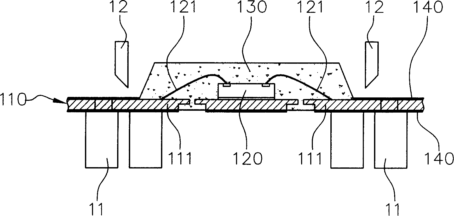
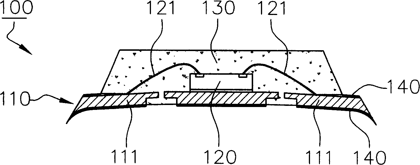
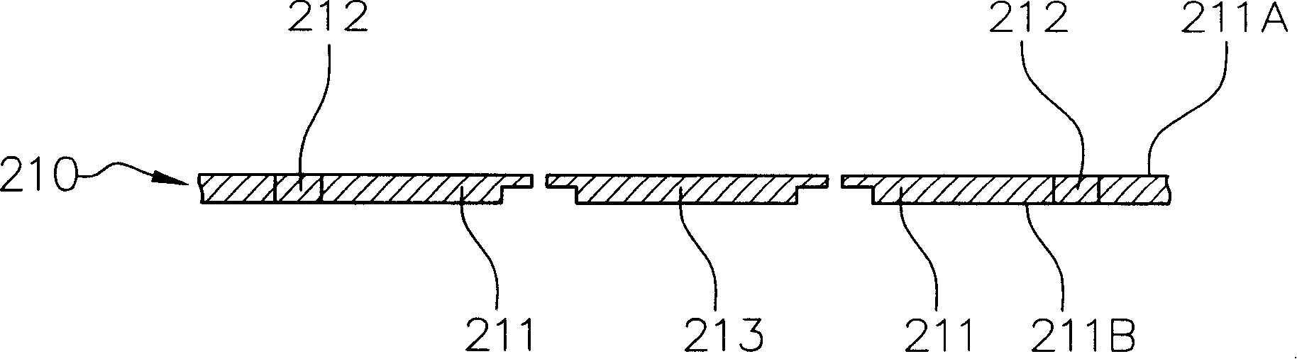
[0066] In a first embodiment of the invention, see Figures 3A to 3G Shown is a schematic cross-sectional view of a punching-out leadless package structure in the manufacturing process according to the first embodiment of the present invention, and discloses a manufacturing method of a punching-out leadless package structure. Figure 4 It is a schematic top view of a lead frame used in the punched leadless package structure, and a schematic top view of a lead frame used in the manufacturing process.

[0067] Fir...


PUM


Abstract

The invention relates to a blanking-type packaging structure without outer pins and a manufacturing method thereof. The manufacturing method of the blanking-type packaging structure without outer pins comprises the following steps: providing a lead frame with a plurality of carrier units, wherein each carrier unit internally forms a plurality of pins, disposing a plurality of wafers to the lead frame, wherein the wafers are electrically connected to the pins, forming a plurality of glue sealing bodies on the carrier units and combining the pins, performing one step of semi-blanking to form a plurality of half-concave nicks on the pins along the outer periphery of the glue sealing bodies, performing one step of electric plating to form an electric plating layer on the exposed surface of the half-concave nicks of the pins and performing one step of complete plating for cutting off the pins along the half-concave nicks to be divided into individual glue sealing bodies. The invention can resolve the problems that the pins of the blanking-type packaging structure without outer pins are torn off, dropped down with rough edges and the like in the single planking process, and the invention can increase the excellent rate of the process and even increase the plating area of the pins, thereby being quite suitable for utility.

Description

technical field [0001] The present invention relates to a singulation of semiconductor packaging technology, and in particular to a method that can solve the problems of pin peeling, falling and burrs in the punching-out pinless packaging structure during the manufacturing process, and The punching-type no-outer-lead packaging structure and its manufacturing method can improve the process yield and increase the plating area of ​​the leads. Background technique [0002] In the current semiconductor packaging manufacturing technology, it is quite common and economically efficient to first integrate a plurality of carrier units on a substrate for the packaging process. After most of the packaging process is completed, the monomers are separated to separate a plurality of semiconductor packaging structures. For example, this is the case when a leadless IC package is produced using a lead frame as a base material, and the monomers are separated at the end of the manufacturing pr...

Claims


Application Information

Patent Timeline
Patent Type & Authority Applications(China)
IPC IPC(8): H01L21/60H01L23/495
CPCH01L2224/92247H01L24/97H01L2224/48091H01L2224/73265H01L2224/32245H01L2224/48247H01L2224/97
Inventor 林鸿村
Owner CHIPMOS TECH INC
Why Eureka
Try Eureka