Circuit board and manufacturing method thereof

A production method and circuit board technology, which is applied in the fields of printed circuit manufacturing, printed circuit, printed circuit components, etc., can solve the problems of reduced yield rate of circuit boards, and achieve the effect of improving yield rate and reducing skip plating or missed plating

Active Publication Date: 2022-03-15
UNIMICRON TECH CORP
View PDF8 Cites 0 Cited by
  • Summary
  • Abstract
  • Description
  • Claims
  • Application Information

AI Technical Summary

Problems solved by technology

However, in the electroplating process, skip plating or skip plating often causes the yield rate of the circuit board to decrease.

Method used


Image

  • Circuit board and manufacturing method thereof
  • Circuit board and manufacturing method thereof
  • Circuit board and manufacturing method thereof

Examples


Embodiment Construction

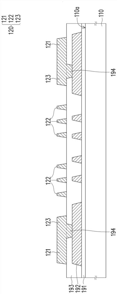
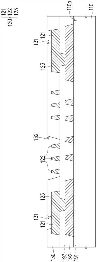
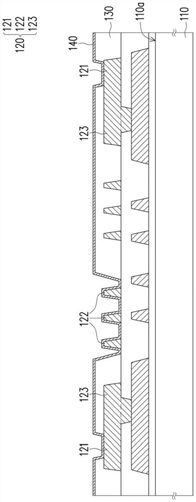
[0066] The aforementioned and other technical contents, features and effects of the present invention will be clearly presented in the following detailed descriptions of the embodiments with reference to the accompanying drawings. The directional terms mentioned in the following embodiments, such as "upper", "lower", "top", "bottom", etc., are only referring to the directions of the accompanying drawings. Accordingly, the directional terms used are illustrative, not limiting, of the invention.

[0067] In the detailed description of various embodiments, terms such as "first", "second", and "third" may be used to describe different elements. These terms are only used to distinguish one element from another, but in the structure, these elements should not be limited by these terms. For example, a first element could be termed a second element, and, similarly, a second element could be termed a first element without departing from the scope of the present inventive concept. In ...


PUM


Abstract

The invention provides a circuit board and a manufacturing method thereof. The circuit board includes a substrate, a patterned conductive layer, a patterned insulating layer, a conductive terminal and a dummy terminal. The patterned conductive layer is located on the substrate. The patterned insulating layer is located on the substrate and covers at least part of the patterned conductive layer. The conductive terminal is located on the patterned conductive layer and has a first top surface. The dummy terminal is located on the patterned conductive layer and has a second top surface. There is a first height between the first top surface and the substrate, a second height between the second top surface and the substrate, and the first height is greater than the second height.

Description

technical field [0001] The invention relates to an electronic component and a manufacturing method thereof, in particular to a circuit board and a manufacturing method thereof. Background technique [0002] The electroplating process is often used in the manufacturing method of the circuit board. However, during the electroplating process, skip plating or skip plating often causes a decrease in the yield of the circuit board. Contents of the invention [0003] The invention provides a circuit board and a manufacturing method thereof, which have better yield. [0004] The circuit board of the present invention includes a substrate, a patterned conductive layer, a patterned insulating layer, conductive terminals and dummy terminals. The patterned conductive layer is located on the substrate. The patterned insulating layer is located on the substrate and covers at least part of the patterned conductive layer. The conductive terminal is located on the patterned conductive ...

Claims


Application Information

Patent Timeline
Patent Type & Authority Patents(China)
IPC IPC(8): H05K3/18H05K1/11
CPCH05K3/18H05K1/11
Inventor 杨凯铭林晨浩
Owner UNIMICRON TECH CORP
Why Eureka
Try Eureka