Semiconductor integrated circuit

An integrated circuit and semiconductor technology, applied in the field of semiconductor integrated circuits, can solve the problems of reduced threshold voltage of MOS transistors and increased sub-threshold leakage current, etc., and achieves the effects of high manufacturing yield, reduced operating power consumption and changes in signal delay amount.

Inactive Publication Date: 2008-07-30
RENESAS ELECTRONICS CORP
View PDF1 Cites 10 Cited by
  • Summary
  • Abstract
  • Description
  • Claims
  • Application Information

AI Technical Summary

Problems solved by technology

[0002] Due to the short channel effect brought about by the miniaturization of semiconductor devices, the threshold voltage of MOS transistors decreases, and the subthreshold leakage current increases significantly

Method used


Image

  • Semiconductor integrated circuit
  • Semiconductor integrated circuit
  • Semiconductor integrated circuit

Examples


Embodiment Construction

[0041] "Representative Implementation Mode"

[0042] First, representative embodiments of the technical solutions disclosed in the present application will be briefly described. The reference numerals put in parentheses and referred to in the brief description of the representative embodiments are merely examples of members included in the concept of the constituent elements to which the numerals are attached.

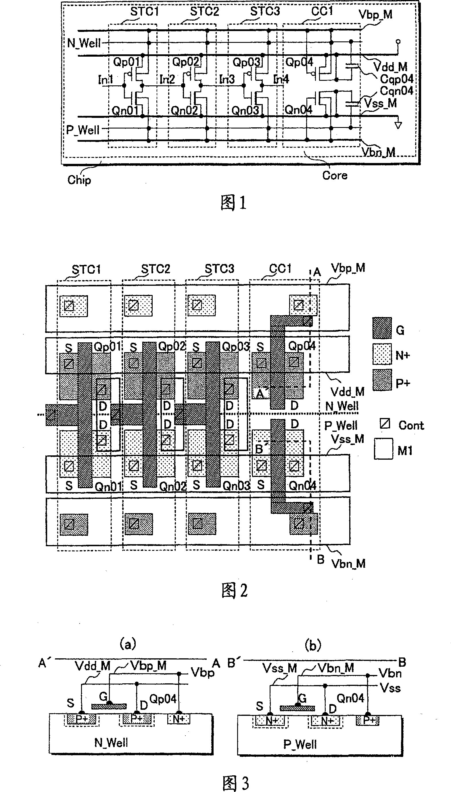
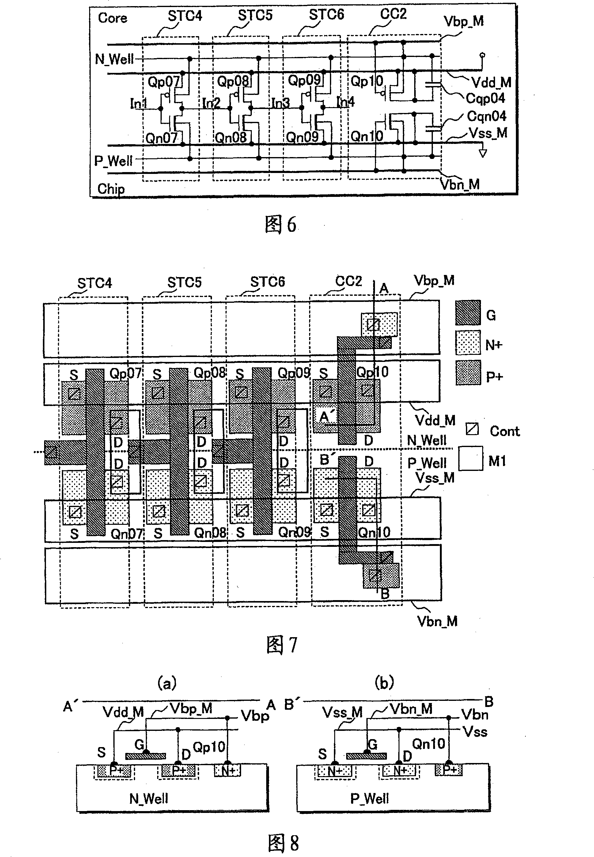
[0043] (1) A semiconductor integrated circuit (Chip) according to a typical embodiment of the present invention includes CMOS circuits (ST1, ST2, ST3) for processing an input signal (In1), and additional chips manufactured by the same manufacturing process as the above-mentioned CMOS circuits. Capacitor circuit (CC1). The above CMOS circuit includes PMOS (Qp01, Qp02, Qp03) with N well (N_Well) and NMOS (Qn01, Qn02, Qn03) with P well (P_Well), and the above additional capacitance circuit includes an additional PMOS (Qp04) with N well and additional NMOS (Qn04) with P-...


PUM


Abstract

The present invition provides a semiconductor integrated circuit. A substrate bias technique is used in an active mode enabling a high yield, and an operating consumption power and the fluctuation of a signal delay in signal processing are reduced in the active mode. The additional PMOS and NMOS of the additional capacitance circuit are produced in the same production process as the PMOSs and the NMOSs of the CMOS circuits. The gate capacitance of the additional PMOS is coupled between the power supply wiring and the N well and the gate capacitance of the additional NMOS is coupled between the ground wiring and the P well. The noise on the power supply wiring is transmitted to the N well through the gate capacitance and the noise on the ground wiring is transmitted to the P well through the gate capacitance. The fluctuation of noise on the substrate bias voltage between the source and the well of PMOS and NMOS of the CMOS circuits is reduced.

Description

technical field [0001] The present invention relates to a semiconductor integrated circuit, and more particularly, to the use of substrate bias technology in an active mode capable of achieving a high manufacturing yield, and to reducing fluctuations in operating power consumption and signal delay of signal processing in the active mode Technology. Background technique [0002] Due to the short-channel effect brought about by the miniaturization of semiconductor devices, the threshold voltage of MOS transistors is lowered, and the subthreshold leakage current is significantly increased. The characteristic below the threshold voltage of a MOS transistor is a subthreshold characteristic, and the leakage current when the MOS silicon surface is in a weak inversion state is called a subthreshold leakage current. As a method of reducing this leakage current, a substrate bias technique is known. Subthreshold leakage current can be reduced by applying a predetermined substrate bia...

Claims


Application Information

Patent Timeline
Patent Type & Authority Applications(China)
IPC IPC(8): H01L27/092H01L23/522H03K17/687
CPCH03K19/0008H03K2217/0018H01L21/8238
Inventor 长田健一山冈雅直小松成亘
Owner RENESAS ELECTRONICS CORP
Why Eureka
Try Eureka