Inductor device for multiband radio frequency operation

An inductor, multi-band technology, applied in the direction of inductors, printed inductors, fixed inductors, etc., can solve the problems of differential signal path noise, no significant saving of die area, etc., to achieve the effect of saving die area

Inactive Publication Date: 2008-08-27
NOKIA CORP
View PDF0 Cites 28 Cited by
  • Summary
  • Abstract
  • Description
  • Claims
  • Application Information

AI Technical Summary

Problems solved by technology

The problem with prior art inductors is that prior art inductors (single-ended devices) are utilized in differential operation and the switching creates noise on the differential signal path
In addition, existing techniques do not provide significant savings in die area

Method used


Image

  • Inductor device for multiband radio frequency operation
  • Inductor device for multiband radio frequency operation
  • Inductor device for multiband radio frequency operation

Examples


Embodiment Construction
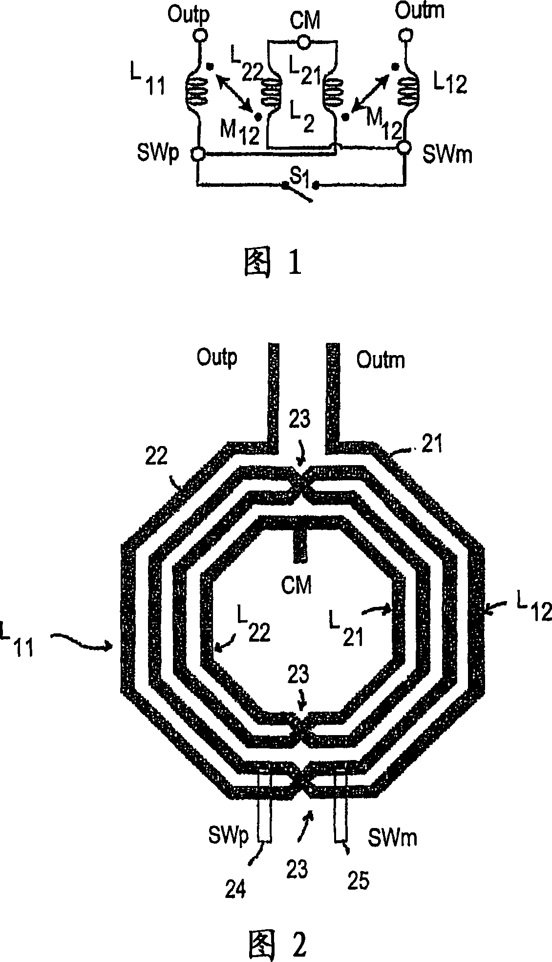
[0032] In Fig. 1, the basic idea of ​​the invention is illustrated by way of example. The inductance of the monolithic planar inductor is distributed to the smaller inductor part L 11 , L 21 , L 22 and L 12 middle. Middle inductor part L 21 and L 22 The node CM between is the common-mode point of the inductor device, which is usually connected to signal ground (for example, to the supply voltage V CC or ground). Inductor part L 21 and L 11 The nodes Outm and Outp at the outer ends of are differential outputs, eg, the output nodes of amplifier devices at the interface of the device itself and subsequent devices (eg, the input stage of a mixer). Middle inductor part L 22 and the external inductor part L 11 between node SWp, and the middle inductor part L 21 and the external inductor part L 12 The node SWm in between is the node at which the short circuit switch function is implemented by a short circuit or bypass switch device S1 connected between nodes SWp and SWm....


PUM


Abstract

The inductance of a monolithic planar inductor is distributed into smaller inductor portions (L11, L21, L22, L12). The smaller inductor portions (L11, L21, L22, L12) are provided in a cascode configuration in a manner that causes inductor to function as a differential inductor device. The node (CM) between the immediate inductor portions (L21, L22 is a common-mode point of the inductor device, which is typically connected to the signal ground. The nodes (Outm,Outp) at the outer ends of the inductor portions (L12,L11 are differential outputs, e.g. output nodes of an amplifier device at the interface of the device itself and the following device (e.g. input stage of a mixer). Some of the inductor portions are arranged to be symmetrically by-passed or shortcut (S1 ) in relation to the common point in one or more steps for operation in one or more higher radio frequency band. By means of the switchable symmetric shortcut, a controllable inductance step can be provided. The common-mode signal is affected the same inductance regardless of the controlled condition.

Description

technical field [0001] The present invention relates to radio frequency (RF) circuits, and in particular to integrated circuits for multiband radio frequency (RF) operation. Background technique [0002] The future trend of multipurpose Radio Frequency Integrated Circuits (RFIC) implementations with multiple simultaneous systems and frequency bands in telecom services is indisputable. New frequency allocations combined with frequency bands acquired from obsolete commercial systems or government and military agencies have created a very fragmented wireless interface. This is a requirement that is setting the demand for RFIC engines with increased complexity and die area consumption. The overall degree of separated RF signal paths in a multipurpose RFIC can be high and will certainly increase in the future. For example, a mobile phone's RFIC may need to support GSM800, GSM1800, GSM1900, CDMA2000, European WCDMA, American WCDMA, WLAN, GPS, and DVB radio interfaces. In direct...

Claims


Application Information

Patent Timeline
Patent Type & Authority Applications(China)
IPC IPC(8): H01F21/12H01F27/28H01FH01F17/00
CPCH03F2203/45386H01F17/0006H01F2021/125H03F3/45098H01F2017/0046
Inventor J·J·埃克基南
Owner NOKIA CORP
Why Eureka
Try Eureka