Organic electroluminescence display device
A display device, organic technology, applied in the direction of electrical components, circuits, electrical solid devices, etc., can solve problems such as deterioration of organic films, and achieve the effects of high contrast, increased volume, and good display characteristics
- Summary
- Abstract
- Description
- Claims
- Application Information
AI Technical Summary
Problems solved by technology
Method used
Image
Examples
Embodiment 1
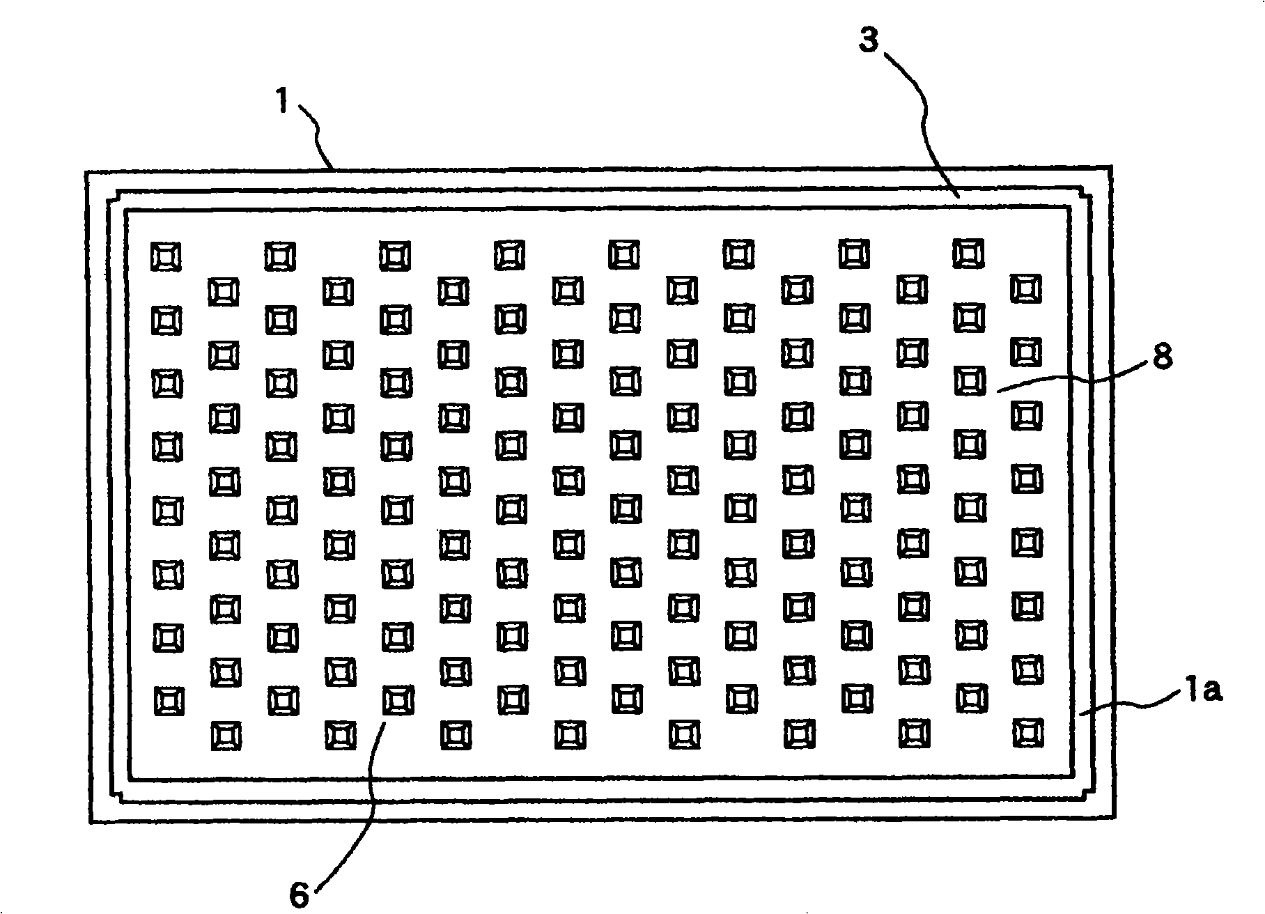
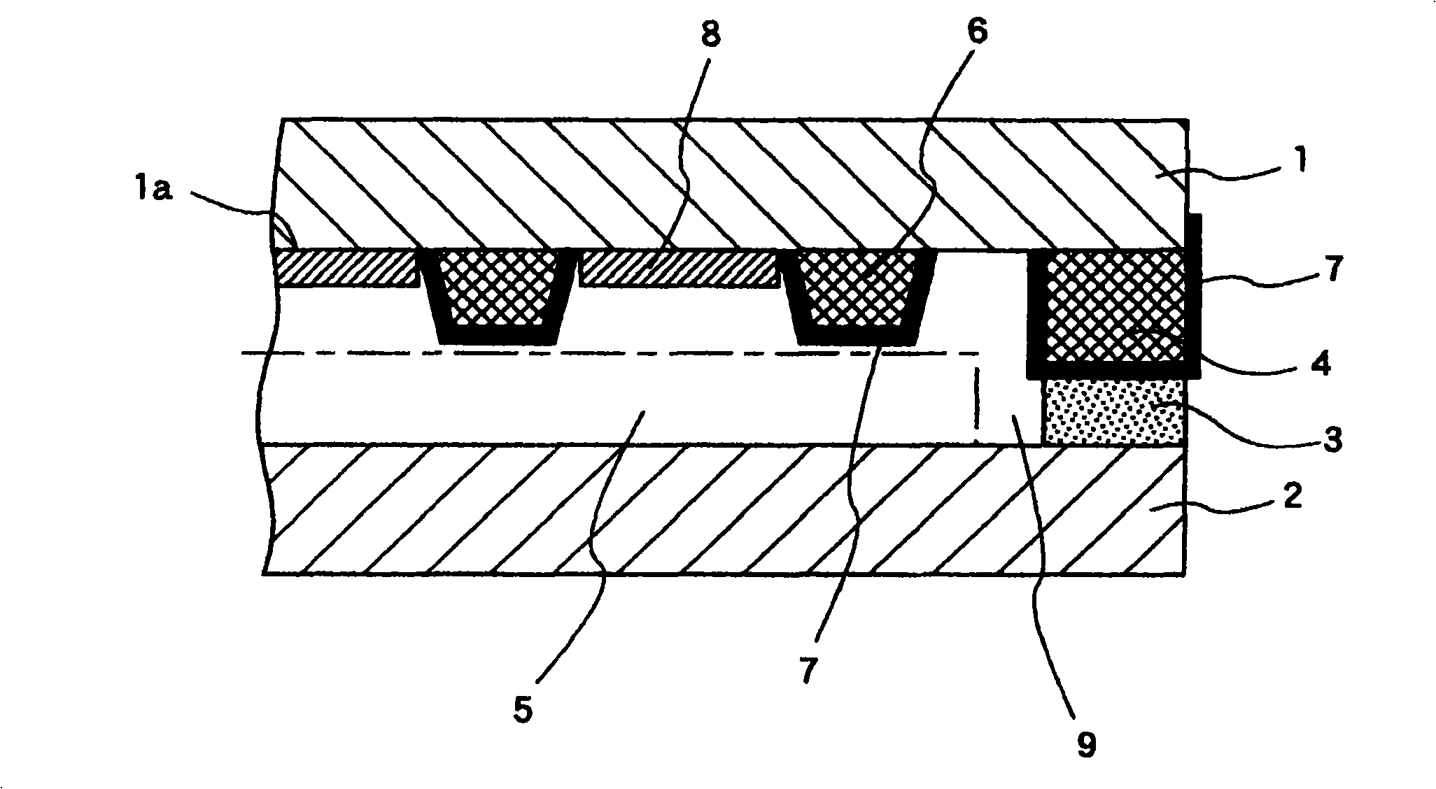
[0039] Figure 1 to Figure 5 It is a schematic diagram illustrating a schematic structure of an embodiment of the organic EL display device of the present invention, figure 1 is a cross-sectional view parallel to the light exit direction, figure 2 is along figure 1 A sectional view of the A-A line, image 3 is zoomed in figure 1 A section view of a part of Figure 4 Yes figure 1 Cross-sectional view of the light-emitting element side, Figure 5 It is an enlarged cross-sectional view of an organic EL layer.
[0040] exist Figure 1 to Figure 5 Among them, reference numeral 1 is a sealing substrate, 2 is an element substrate, 3 is a sealing material, 4 is a side wall, 5 is a light emitting element part, 6 is a spacer, 7 is an inorganic insulating film, 8 is a dry material, and 9 is a sealed space. The above-mentioned sealing substrate 1 is made of, for example, a glass material, and is bonded to an element substrate 2 , which will be described in detail later, via a...
Embodiment 2
[0054] Image 6 It is a schematic cross-sectional view for explaining the schematic structure of another embodiment of the organic EL display device of the present invention, and the same reference numerals are assigned to the same parts as those in the above-mentioned figures.
[0055] In Example 2, such as Image 6 As shown, in addition to the surface of the spacer 6 , the above-mentioned inorganic insulating film 7 is disposed on the inner surface 1 a on the back side of the desiccant 8 . The organic EL display device of Example 2 has the feature of being able to further reduce outgassing.
Embodiment 3
[0057] Figure 7 It is a schematic diagram for explaining the schematic structure of still another embodiment of the organic EL display device of the present invention, Figure 7 (a) shows a cross-sectional view of a columnar spacer, Figure 7 (b) is a cross-sectional view of a spherical (bead) spacer, and the same reference numerals are assigned to the same parts as in the above-mentioned figures.
[0058] First, in Figure 7 In the embodiment shown in (a), the spacer 6 is made of, for example, a columnar spacer 61 shaped into a columnar shape from silicon dioxide, resin, etc., and the spacer 61 is arranged so that the bonding member 10 such as an adhesive resin is interposed therebetween. The state of being dispersed on the inner surface 1a of the sealing substrate 1 is fixed.
[0059] On the other hand, in Figure 7 In the embodiment shown in (b), the spacer 6 is made of, for example, a spherical spacer 62 shaped into a spherical shape (bead) from silicon dioxide, resin...
PUM
 Abstract
Description
Claims
Application Information


