

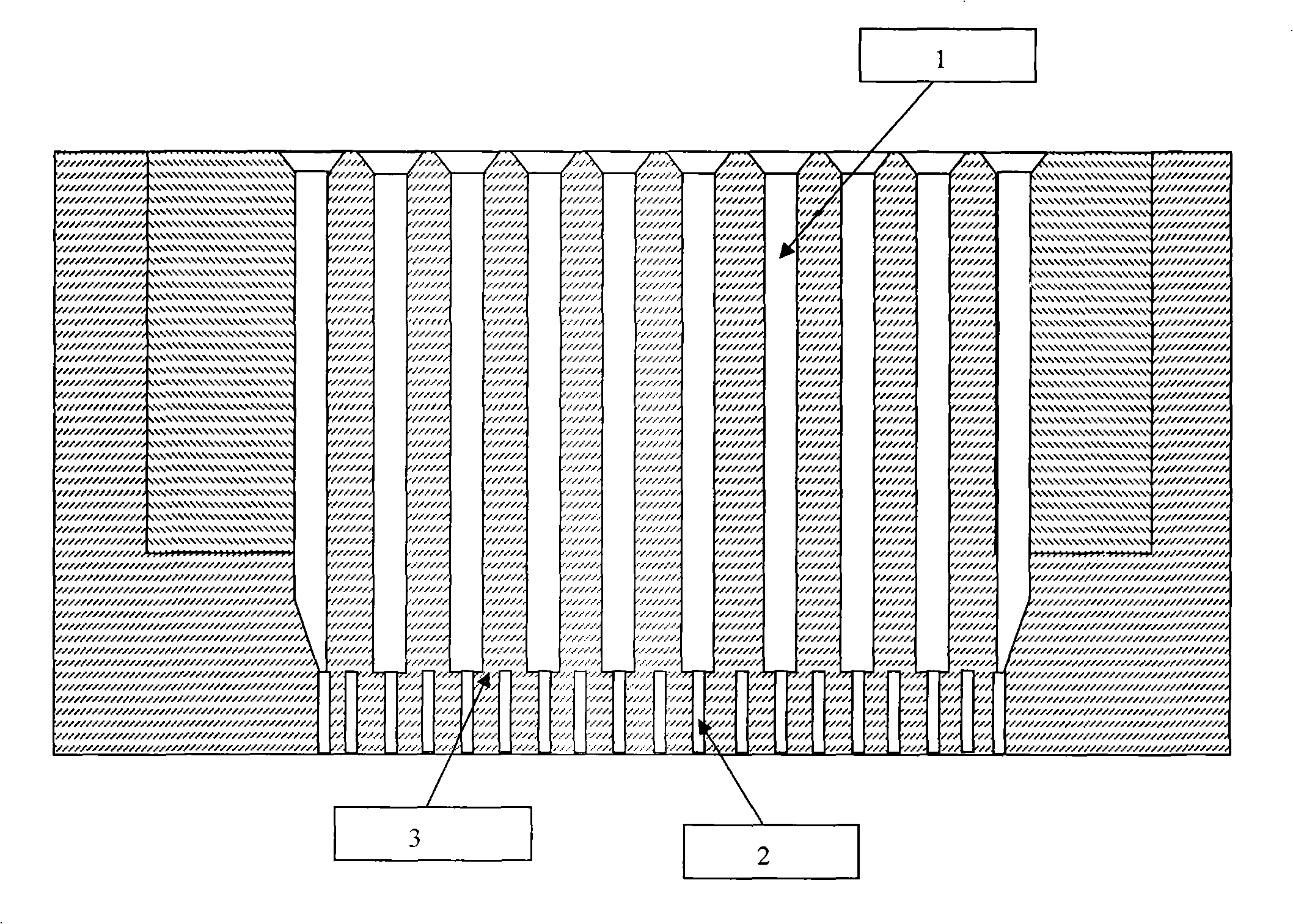
High density holes thin wall honeycomb ceramic extrusion mold and manufacturing method thereof
A manufacturing method and technology of honeycomb ceramics, applied in ceramic extrusion dies, electrolysis process, electroforming, etc., can solve the problems that the mold has no practical value, the lattice wall cannot be reduced, and the hole density has not increased, and the hardness is large. , Improve the service life and reduce friction
- Summary
- Abstract
- Description
- Claims
- Application Information
AI Technical Summary
Problems solved by technology
Method used
Image

Examples
Embodiment 1
[0021] Embodiment 1 Electroless nickel plating alloy, (design is 600 order, grid wall thickness is 0.12mm, and the grid wall thickness of semi-finished product is 0.18mm) the semi-finished product mold that will produce is put into the cleaning liquid that configures containing surfactant in turn Clean the mold thoroughly with ultrasonic vibration and pure water to ensure that no dirt and rust remain on the surface of the mold. Hang the cleaned mold in the circulating chemical plating solution. The temperature of the chemical plating solution should be controlled between 40°C and 100°C. The speed of chemical plating will increase with the increase of temperature. When the surface of the mold is uniform After coating a layer of nickel alloy with a thickness of 30um, the finished mold is taken out of the plating solution, and the residual liquid on the surface is washed away with water, so that a finished mold with a 600-mesh grid and a wall thickness of 0.12mm is completed. .Th...
Embodiment 2
[0022] Example 2 Electroless plating of silicon carbide: the processed 900-purpose semi-finished mold (the diameter of the mud guide hole is 1.0 mm and the width of the cutting groove is 0.15 mm, and the design requirements of the mold are that the diameter of the mud guide hole is 0.93 mm and the width of the cutting groove is 0.08 mm ) is cleaned according to the same cleaning method as in Example 1, and then the mold is put into the plating solution according to the above same method for coating treatment. The plating solution used here is due to the addition of nanometer silicon carbide in the conventional alloy steel plating solution , so that when the surface of the mold is covered with the alloy coating, nanometer silicon carbide particles will be deposited and embedded in the alloy steel coating at the same time. The residual liquid is cleaned up, so that a mold with a 900 mesh grid wall thickness of 0.08mm is produced. In order to increase the strength of the mold, th...
Embodiment 3
[0023] Example 3 Vapor deposition of tungsten carbide: Clean the processed semi-finished mold with 600 mesh and grid wall thickness of 0.15mm according to the same method as in the above example, and then put the semi-finished mold into the airtight equipment for special vapor deposition treatment. On the object table, set the deposition time according to the parameters of the coating thickness of 25um, and then turn on the equipment according to the conventional vapor deposition method. After the equipment stops running, take out the finished mold, and the finished mold becomes a 600-mesh grid with a wall thickness of 0.1mm . The strength of the mold produced by this method is higher than that of the above example, but the mold is prone to deformation.
PUM
| Property | Measurement | Unit |
|---|---|---|
| Thickness | aaaaa | aaaaa |
Abstract
Description
Claims
Application Information