Electroplating device for printed breadboard

A technology for printed circuit boards and electroplating devices, used in jewelry and other directions, can solve problems such as affecting product processing quality, inability to accurately control line width tolerance, and uneven copper plating thickness.

Inactive Publication Date: 2008-09-10
SHENZHEN FASTPRINT CIRCUIT TECH
View PDF0 Cites 13 Cited by
  • Summary
  • Abstract
  • Description
  • Claims
  • Application Information

AI Technical Summary

Problems solved by technology

In the electroplating process of printed circuit boards, the surface conductor copper has certain standard requirements, and because the distribution of power lines in the electroplating tank is uneven, especially the distribution of power lines around the entire electroplating window is relatively dense, so copper plating around

Method used


Image

  • Electroplating device for printed breadboard
  • Electroplating device for printed breadboard
  • Electroplating device for printed breadboard

Examples


Embodiment Construction

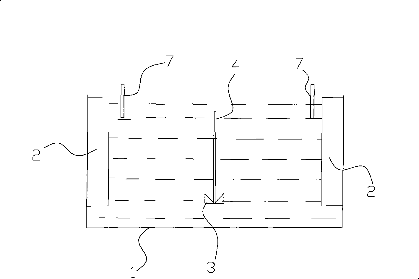
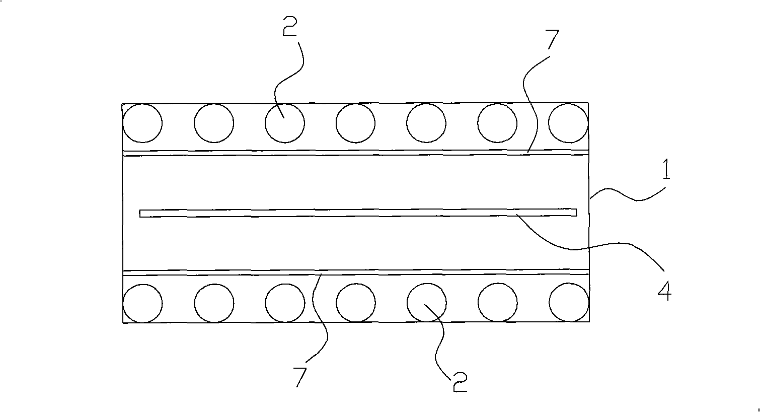
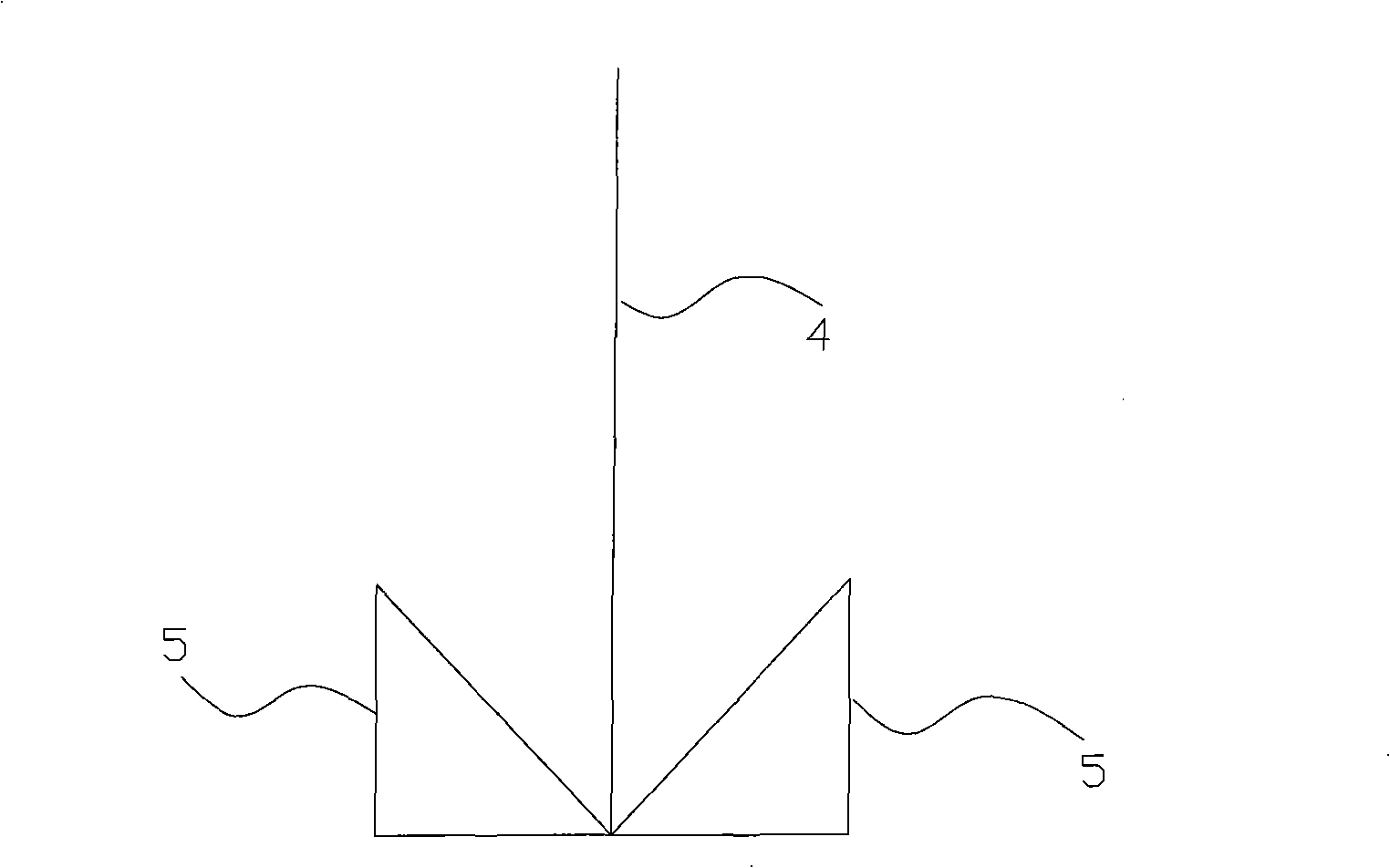
[0021] Such as Figure 1 to Figure 6 As shown, an electroplating device for a printed circuit board is provided with two opposite anodes 2 in the electroplating tank 1, and the two anodes 2 are electrically connected to the positive electrode, and the two anodes 2 are arranged between the two anodes 2 in the electroplating tank 1 There is a floating tank 3, on which a circuit board 4 connected to the negative electrode is arranged; the floating tank 3 includes two side plates 5, the circuit board 4 is positioned between the two side plates 5, and Both are provided with side plate holes 6.

[0022] Wherein, the electroplating tank 1 is provided with a flybar 10 (i.e. a fixed beam), and a hanger 9 is arranged on the flybar 10, and a plurality of circuit boards are suspended on the hanger 9; two side plates 5 are parallel to the circuit board 4 , the side plate holes 6 on each side plate 5 are multiple to form a row of holes, and among the side plate holes 6 on the side plates 5...


PUM


Abstract

The invention discloses an electroplating device for a printed circuit board, wherein, two opposite anodes are arranged inside an electroplating bath and electrically connected with a positive electrode; a floating trough is arranged between the two anodes in the electroplating bath; the printed circuit board which is connected with a negative electrode is arranged on the floating trough; the floating trough comprises two side plates; the circuit board is positioned between the side plates; and side plate holes are uniformly arranged on the two side plates. The electroplating device for the printed circuit board readjusts a power line in the electroplating bath, thereby electroplating of the circuit board is more uniform and the electroplating effect is good.

Description

technical field [0001] The invention relates to an electroplating device for a printed circuit board. Background technique [0002] Today's electronic products have gradually developed in the direction of light, thin, and small, which makes the integration of electronic products continue to increase. As printed circuit boards for connecting components in electronic products, their conductive patterns and via holes are becoming more and more dense. The conductor density, spacing and via hole diameter are getting smaller and smaller, which brings severe challenges to the production of printed circuit boards. In the electroplating process of printed circuit boards, the surface conductor copper has certain standard requirements, and because the distribution of power lines in the electroplating tank is uneven, especially the distribution of power lines around the entire electroplating window is relatively dense, so copper plating around the circuit board Thicker than the center ...

Claims


Application Information

Patent Timeline
IPC IPC(8): C25D7/00C25D3/38
Inventor 刘湘龙
Owner SHENZHEN FASTPRINT CIRCUIT TECH
Why Eureka
Try Eureka