Semiconductor device and method of manufacturing same

A semiconductor and housing technology, which is applied in the fields of semiconductor/solid-state device manufacturing, semiconductor devices, and semiconductor/solid-state device components, etc., can solve the problems of difficulty in automatic operation of assembly robots, dependence, and longer order-to-delivery period, etc. Achieve the effect of improving wire bonding efficiency and high bonding strength

Active Publication Date: 2008-09-10
FUJI ELECTRIC CO LTD
View PDF1 Cites 29 Cited by
  • Summary
  • Abstract
  • Description
  • Claims
  • Application Information

AI Technical Summary

Problems solved by technology

Furthermore, external terminals 6 having different shapes (refer to Figure 13 (a), (b)) It is actually difficult to automate the assembly robot to install it at a designated position in the molding die in a manner c...

Method used


Image

  • Semiconductor device and method of manufacturing same
  • Semiconductor device and method of manufacturing same
  • Semiconductor device and method of manufacturing same

Examples


Embodiment 1

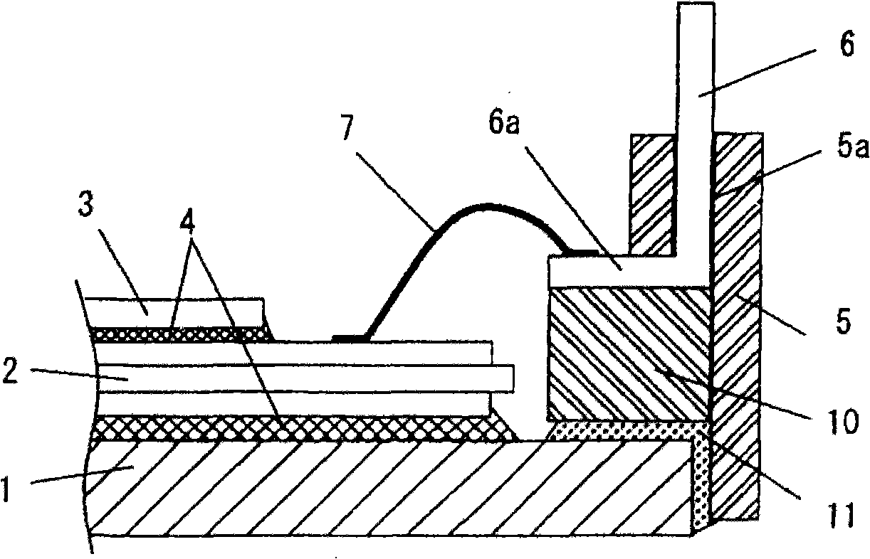
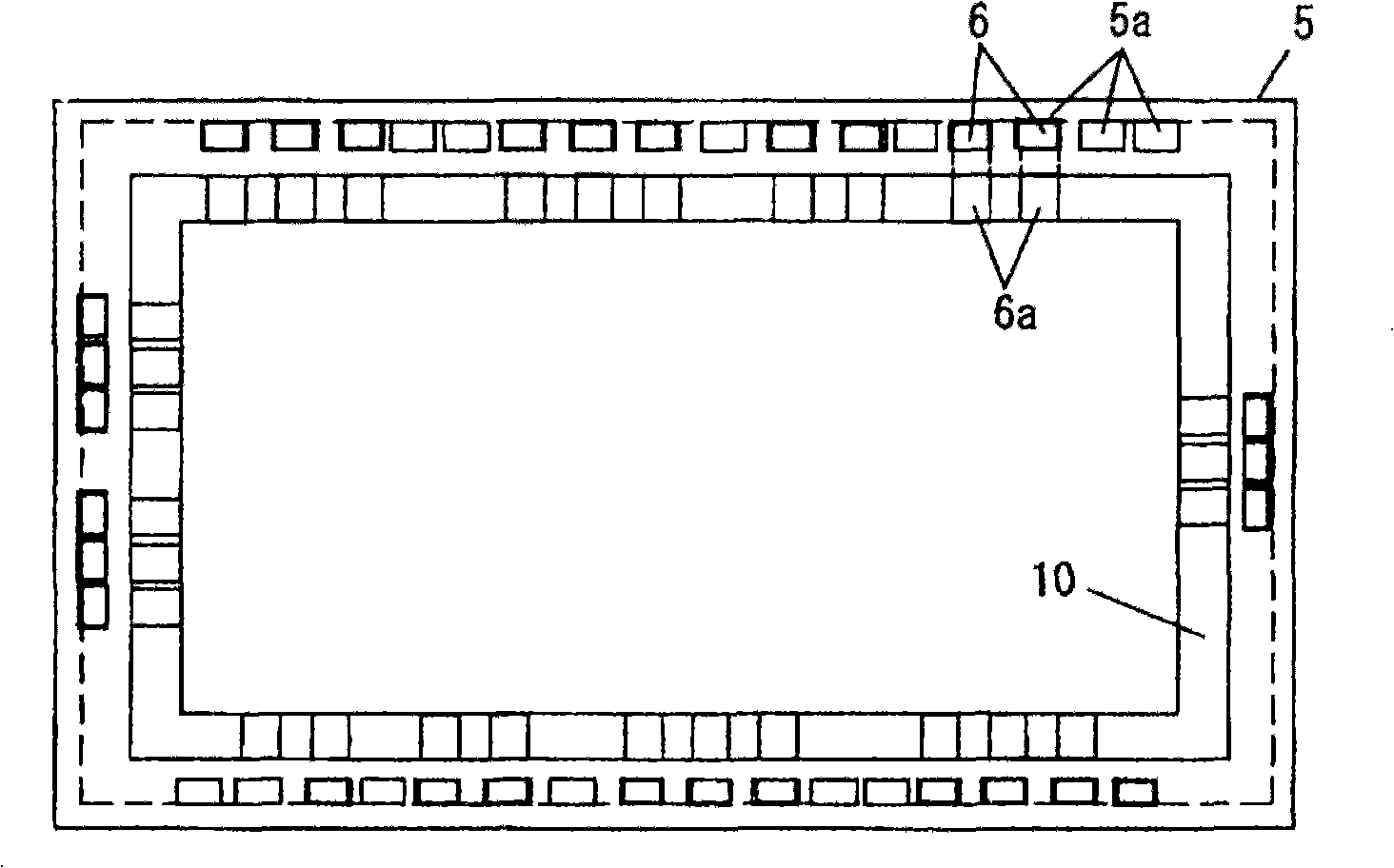
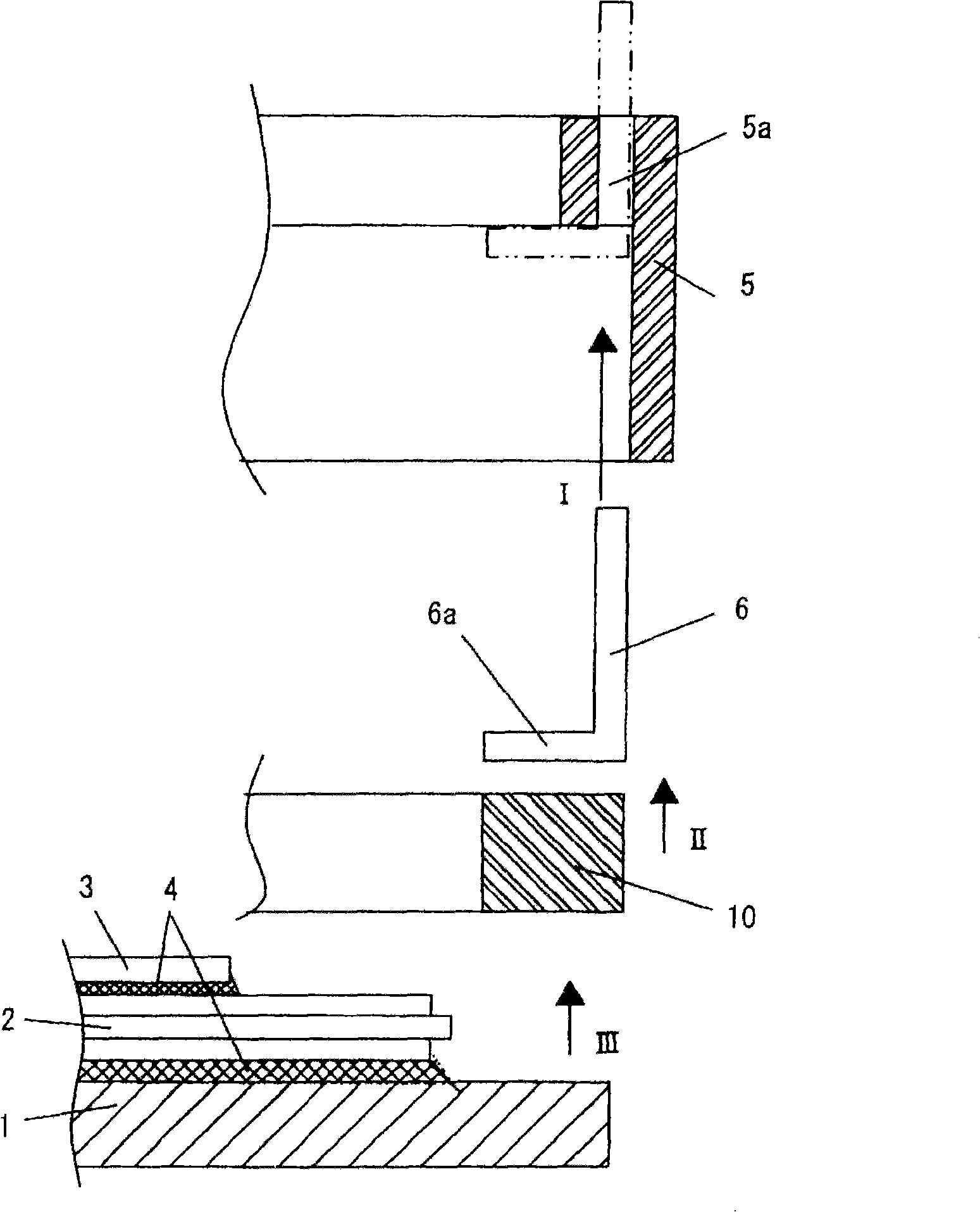
[0056] First, use figure 1 , figure 2 The assembly structure of the package according to the embodiment of the present invention will be described. This example is the same as Figure 11 Compared with the terminal-integrated structure in which the external terminal 6 is insert-molded on the peripheral resin case 5 such as the above-mentioned conventional structure, it is different in the following points. That is, in the illustrated embodiment, along the peripheral wall of the peripheral resin case 5 , terminal attachment holes 5 a are formed in advance at a plurality of positions aligned at predetermined intervals. Wherein, the terminal mounting hole 5a is formed by setting a center corresponding to the terminal mounting hole on the molding die during the molding process of the peripheral resin case 5 and then punching it. In addition, when assembling the package, the hole for mounting the external terminal 6 is selected from the above-mentioned terminal mounting hole 5a...

Embodiment 2

[0070] Next, use Figure 6 ~ Figure 10 , a second embodiment that further improves the package structure of the above-mentioned embodiment 1 will be described. In this embodiment, the following structures are added to the peripheral resin case 5 and the terminal fastening frame 10 . That is, a concave-convex step portion 5 b is formed on the upper surface side along the peripheral wall portion of the peripheral resin case 5 . The concave-convex step portion 5b is formed so that the recessed portion 5b-1 is located in the middle of the adjacent terminal attachment holes 5a to match the arrangement pitch of the terminal attachment holes 5a. Thus, if Figure 10 As shown in (a), a creepage distance d larger than the space distance is formed between the external terminals 6 drawn outward from the peripheral resin case 5 , and high insulation resistance can be ensured.

[0071] On the other hand, regarding the terminal fastening frame 10, press-fit protrusions 10a having a V-shap...


PUM


Abstract

The present invention provides a semiconductor device which has a packaging structure of the improved packaging piece. The substrate packaging piece which is composed of a metal base for heat radiation, an insulation circuit board and a semiconductor chip is assembled with a peripheral resin casing. The L-shaped legs of the external terminals which are arranged on the surrounding wall of the peripheral resin casing are leaded to the inner side of the casing. A joint conducting wire is connected between the leg part and the conductor pattern of the insulation circuit board. In the semiconductor device with the structure, the peripheral resin casing is beforehand punched at the surrounding wall to form a plurality of terminal installing holes, and the necessary external terminals are installed in the terminal installing holes. Hereon, the terminal installing holes are designed and formed with a mode which can be corresponding with the arrangement of all device types and terminals with different standards. When the packaging piece is installed, the terminal installing holes which are selected according to the assigned standard are pressed with external terminals necessary for installation.

Description

technical field [0001] The present invention relates to a semiconductor device used in an intelligent power module (IPM: Intelligent Power Module) suitable for an inverter device. Specifically, it relates to a package structure of the semiconductor device and an assembly method thereof. Background technique [0002] first, Figure 11 ~ Figure 13 The assembly structure of the conventional package of the said semiconductor device is shown. exist Figure 11 Among them, 1 is a metal base for heat dissipation made of copper, 2 is an insulating circuit substrate with conductor patterns formed on both sides of the insulating substrate, and 3 is a semiconductor chip mounted on the insulating circuit substrate 2, such as an insulated gate bipolar transistor ( IGBT: Insulated Gate Bipolar Transistor), 4 is the solder bonding layer that is bonded between the metal base 1 and the insulating circuit substrate 2, and between the insulating circuit substrate 2 and the semiconductor chip 3...

Claims


Application Information

Patent Timeline
IPC IPC(8): H01L23/045H01L23/488H01L21/50H01L21/60
CPCH01L2924/01002H01L2924/01014H01L2924/19107H01L24/49H01L2224/48472H01L2924/01005H01L2224/73265H01L2924/01082H01L2924/01013H01L2224/32225H01L2924/01015H01L2924/014H01L2924/01023H01L2224/48091H01L2924/01029H01L2224/48247H01L2224/45124H01L2924/01004H01L2924/16195H01L2924/01006H01L2224/48227H01L2924/01033H01L2224/4911H01L2924/13055H01L2924/1305H01L24/73H01L2924/181H01L2224/49H01L2924/00014H01L2924/00H01L2924/00012
Inventor 吉原克彦丸山力宏茅野政秋望月英司横山元圣西泽龙男杉山智宣
Owner FUJI ELECTRIC CO LTD
Why Eureka
Try Eureka