Image sensor package with grain receiving opening and method of the same

A technology of image sensor and crystal grain, which can be used in electric solid-state devices, semiconductor devices, radiation control devices, etc., and can solve problems such as increased thickness

Inactive Publication Date: 2008-09-10
ADVANCED CHIP ENG TECH INC
View PDF0 Cites 26 Cited by
  • Summary
  • Abstract
  • Description
  • Claims
  • Application Information

AI Technical Summary

Problems solved by technology

Typically, all stacked redistribution layers are formed on the built-up of the die, increasing the thickness of the package and thus conflicting with the need to shrink the chip size

Method used


Image

  • Image sensor package with grain receiving opening and method of the same
  • Image sensor package with grain receiving opening and method of the same
  • Image sensor package with grain receiving opening and method of the same

Examples


Embodiment 1

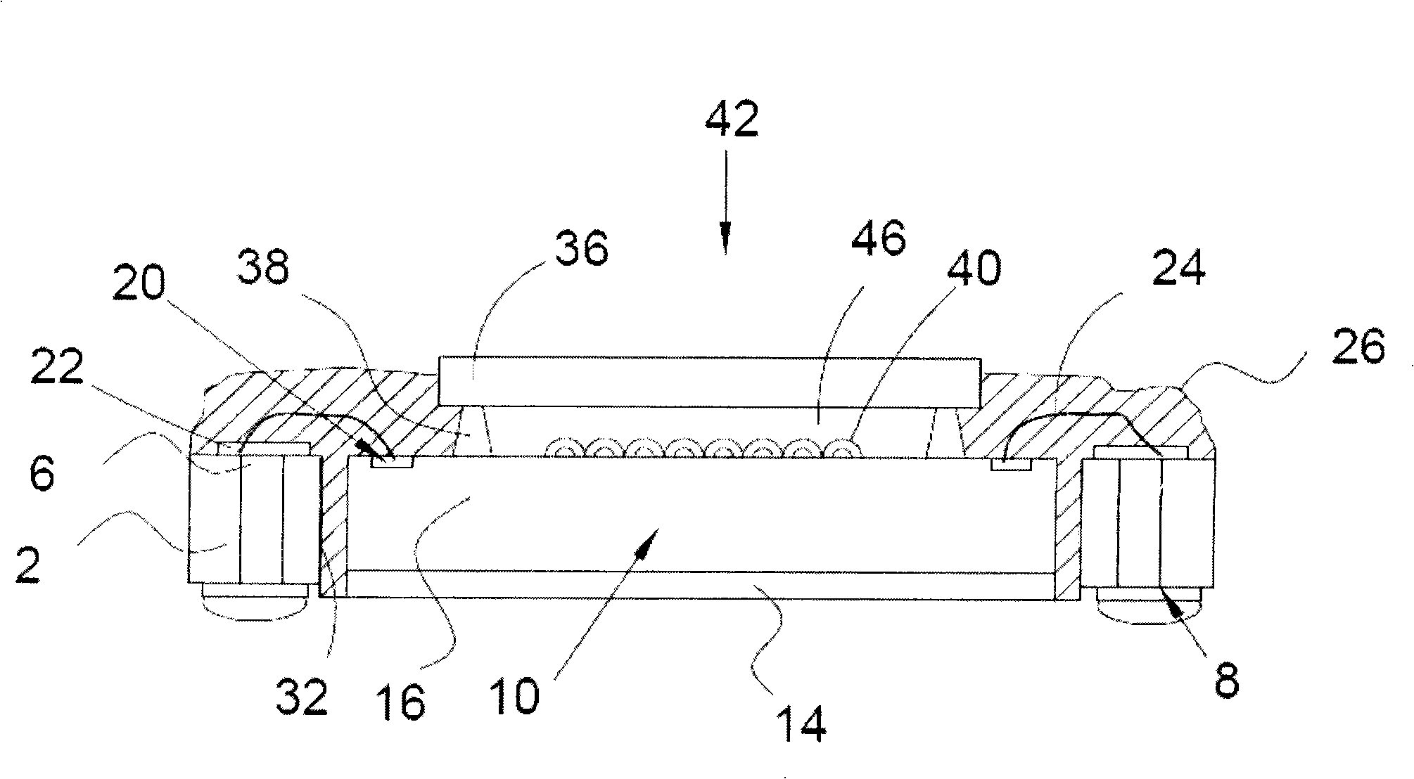
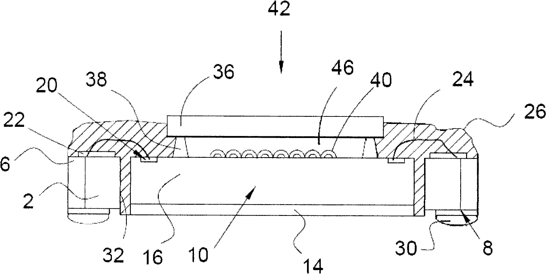
[0040] figure 1 To illustrate a cross-sectional view of a CIS-CSP (CMOS Image Sensor Chip Scale Package) according to an embodiment of the present invention; figure 1 As shown, the structure of the PLP includes a substrate 2 having predetermined die vias 10 and pad (interconnect) vias 6 formed therein to accommodate a die 16; die 16 is preferably an image sensor die A plurality of pad via holes 6 are formed to connect the upper surface and the lower surface of the substrate 2, wherein the pad (interconnection) via holes 6 are surrounded by the substrate 2; a conductive material will be filled into the via holes 6 to conduct The (terminal) pad 8 is positioned on the lower surface of the substrate 2 and is connected to the pad through hole 6 with the conductive material; the conductive wire pad 22 (such as a metal material) is positioned on the upper surface of the substrate 2 and connected to the pad through hole 6. The conductive material is also connected to the pad through ...


PUM


Abstract

The present invention discloses an image sensor package which is provided with the grain accommodating through holes and a method thereof. The image sensor package comprises the following components: a substrate which is provided with a grain through hole and a contact pad through hole structure formed therein, wherein the terminal contact pad is formed at the lower surface of the contact pad through hole structure, and a conductive projection is coupled to the terminal contact pad which is formed on the upper surface of the substrate; a grain which has a micro lens area is provided at the inner part of the through hole of the grain; a bonding wire which is formed on the grain and the substrate, wherein the bonding wire is coupled to the grain and the contact pad of the bonding wire; a transparent panel which is provided on the grain in the through hole of the grain with an adhering mode for generating a clearance between the transparent panel and the grain; and a protecting layer which covers the bonding wire and is filled to the clearance between the edge of the grain and the side wall of the grain through hole of the wafer. The invention is suitable for the packaging of the image sensor.

Description

technical field [0001] The present invention relates to a panel level package (PLP) packaging structure, and in particular to a substrate with die receiving through holes for accommodating image sensors in the panel level package. Background technique [0002] In the field of semiconductor devices, the density of various semiconductor components has been increasing, while the size of the components has been shrinking. In order to adapt to the above situation, the demands on the packaging and interconnection technology of such high-density components are also increasing. Generally speaking, in a flip-chip attachment method, solder bumps are formed on the surface of the die. To form the solder bumps, a solder composite material can be used to pass through a solder mask to produce the desired solder bumps. solder bump pattern. The functions of chip packaging include power distribution, signal distribution, heat dissipation, protection and support, etc.; when semiconductor dev...

Claims


Application Information

Patent Timeline
Patent Type & Authority Applications(China)
IPC IPC(8): H01L27/146H01L23/488H01L23/498H01L23/31H01L21/50H01L21/60H01L21/56
CPCH01L21/6835H01L24/48H01L24/85H01L24/97H01L27/14618H01L27/14627H01L27/14687H01L2224/48091H01L2224/48235H01L2224/8592H01L2924/01004H01L2924/01077H01L2924/01078H01L2924/09701H01L2924/14H01L2924/15153H01L2924/16235H01L2924/18165H01L2924/3025H01L2924/01068H01L2924/10253H01L2924/00014H01L2924/181H01L2924/00H01L2224/45099H01L2224/45015H01L2924/207H01L23/48H01L21/78H01L27/146
Inventor 杨文焜林殿方张瑞贤王东传许献文
Owner ADVANCED CHIP ENG TECH INC
Why Eureka
Try Eureka