Thin-film transistor, manufacturing method for the same and liquid crystal display panel

A technology of thin film transistors and manufacturing methods, which is applied in the direction of transistors, semiconductor/solid-state device manufacturing, electric solid-state devices, etc., can solve problems such as easy leakage currents, achieve enhanced control capabilities, reduce leakage currents, and improve leakage current characteristics.

Inactive Publication Date: 2008-10-15
INNOCOM TECH (SHENZHEN) CO LTD +1
View PDF0 Cites 0 Cited by
  • Summary
  • Abstract
  • Description
  • Claims
  • Application Information

AI Technical Summary

Problems solved by technology

[0018] In order to solve the problem that the thin film transistors in the prior art are prone to leakage current, it is necessary to provide a thin film transistor that can effectively reduce the leakage current

Method used


Image

  • Thin-film transistor, manufacturing method for the same and liquid crystal display panel
  • Thin-film transistor, manufacturing method for the same and liquid crystal display panel
  • Thin-film transistor, manufacturing method for the same and liquid crystal display panel

Examples


Embodiment Construction

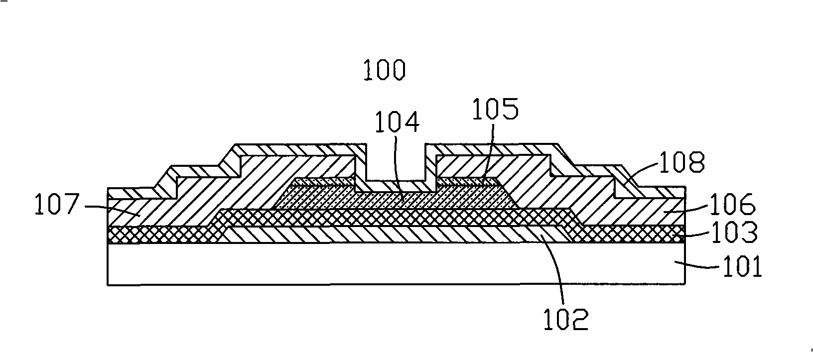
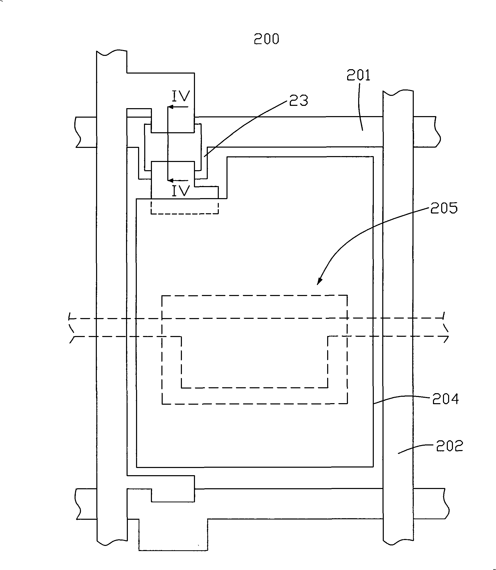
[0031] see image 3 , is a schematic diagram of the structure of the liquid crystal display panel of the present invention. The liquid crystal display panel 200 includes a plurality of rows of scanning lines 201 parallel to each other, a plurality of columns of data lines 202 parallel to each other and insulated from and intersecting with the scanning lines 201, and a plurality of thin films adjacent to the intersections of the scanning lines 201 and the data lines 202 The transistor 23 , a plurality of pixel electrodes 204 and a common electrode 205 opposite to the plurality of pixel electrodes 204 . The pixel electrodes 204 are arranged in a matrix in a region defined by the rows of parallel scanning lines 201 and the columns of parallel scanning lines 201 . The gate of the TFT 23 is correspondingly connected to a scan line 201 , its source is correspondingly connected to a data line 202 , and its drain is correspondingly connected to a pixel electrode 204 .

[0032] When ...


PUM


Abstract

The invention provides a thin film transistor and a manufacturing method thereof. The thin film transistor comprises a substrate, a grid arranged on the surface of the substrate, a grid passivation layer covering the substrate and the grid, a channel region arranged on the surface of the grid passivation layer, a drain electrode and a source electrode covering the grid passivation layer and part of the channel region as well as a conductive film arranged between the drain electrode and the channel region, wherein, the work function of the conductive film is bigger than that of the channel region. The conductive film with higher work function is arranged between the drain electrode and the channel region, the energy barrier value between the drain electrode and the channel region is enhanced so as to effectively improve the drain current characteristic of the thin film transistor. Simultaneously, the invention also provides a liquid crystal display panel which adopts the thin film transistor.

Description

technical field [0001] The invention relates to a thin film transistor, a manufacturing method thereof, and a liquid crystal display panel using the thin film transistor. Background technique [0002] In a thin film transistor liquid crystal display panel, the light transmittance of the display area mainly depends on the voltage difference between the pixel electrode and the common electrode. When the thin-film transistor is turned on, the data voltage is transmitted to the pixel electrode through the turned-on thin-film transistor, and then the thin-film transistor is immediately turned off to keep the charge on the liquid crystal capacitor. If the stored charge is lost at this time, it will cause the voltage of the liquid crystal capacitor to change. , until the new data voltage is input again. Usually, it is necessary to ensure that the change of the liquid crystal capacitor voltage cannot cause the luminance change of the affected display area to exceed one gray scale, ...

Claims


Application Information

Patent Timeline
Patent Type & Authority Applications(China)
IPC IPC(8): H01L29/786H01L21/336H01L27/12G02F1/1362
CPCH01L29/458G02F1/1368H01L29/66765
Inventor 颜硕廷洪肇逸
Owner INNOCOM TECH (SHENZHEN) CO LTD
Why Eureka
Try Eureka