Method for preparing capacitor in semiconductor assembly

A technology for semiconductors and capacitors, which is applied in the field of using a ring-shaped Si3N4 to prepare capacitors in semiconductor components, which can solve difficult problems such as dielectric layer thickness, oxidation resistance reduction, and oxidation

Inactive Publication Date: 2006-06-21
SK HYNIX INC
View PDF0 Cites 0 Cited by
  • Summary
  • Abstract
  • Description
  • Claims
  • Application Information

AI Technical Summary

Problems solved by technology

[0005] However, due to the reduction of the design rules leading to the reduction of the unit cell (Cell) area, the thickness of the dielectric layer (dielectric) is reduced (T eff ) is required to obtain the necessary charge
[0006] As for the conventional N / O dielectric layer, due to the LPCVD method Si 3 N 4 When the thickness is lower than 40 Å, the oxidation resistance will be severely reduced, so the problem that the semiconductor elements located under the capacitor, such as storage nodes and bit-lines (bit-line) are oxidized in the third ONO method occurs, and, It is difficult to make the thickness of the dielectric layer T eff Less than 45 Å, because at thicknesses below 50 Å, leakage current increases and breakdown voltage decreases

Method used


Image

  • Method for preparing capacitor in semiconductor assembly
  • Method for preparing capacitor in semiconductor assembly
  • Method for preparing capacitor in semiconductor assembly

Examples


Embodiment Construction

[0014] Hereinafter, a preferred embodiment of the present invention will be described in detail with reference to the drawings. In the following description and the drawings, the same reference numerals are used to denote the same or similar elements, so repeated descriptions of the same or similar elements in the description are omitted.

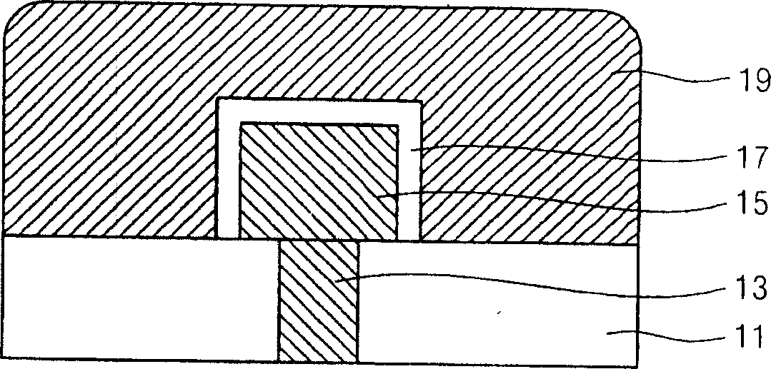
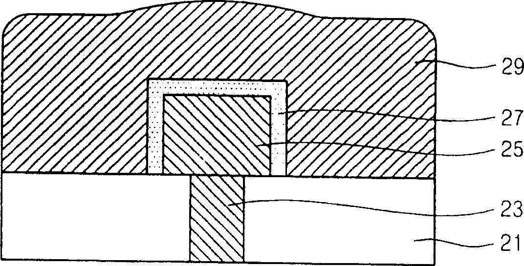
[0015] Such as figure 2 As shown, it relates to a method for manufacturing a capacitor in a semiconductor component of the present invention. The interlayer insulating layer 21 is deposited on a wafer (not shown), in which some elements are formed, and the selective layout pattern of the interlayer insulating layer is scribed to form contact holes (not shown) that can expose part of the semiconductor wafer .

[0016] Next, a contact plug 23 is formed in a contact hole (not shown), and a cylindrical, recessed, or other storage node 25 is formed on the entire surface of the semiconductor wafer.

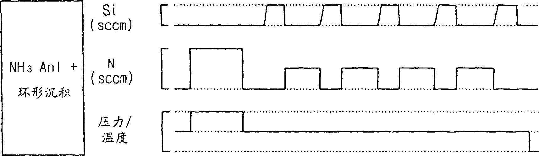
[0017] Then, by the ring Si 3 N 4 Or SiO x N y (W...


PUM


Abstract

The invention provides a method for preparing a capacitor in a semiconductor component, which includes the following steps: forming a storage node electrode on a semiconductor wafer; forming a dielectric layer made of ring-shaped silicon nitride on the storage node electrode; and here The upper electrode is formed on the dielectric layer; the thickness T of the dielectric layer is reduced eff and by using Si 3 N 4 or SiO x N y (where x is between 0.1 and 0.9, and y is between 0.1 and 2) as a dielectric layer to improve leakage current characteristics; as a dielectric layer, it has high oxidation resistance and high dielectric ratio.

Description

Technical field [0001] The invention relates to a method for preparing a capacitor in a semiconductor component, in particular to a method for using a ring-shaped Si 3 N 4 (Or SiO x N y ) To prepare capacitors in semiconductor components. Background technique [0002] Such as figure 1 As shown, the conventional N / O(Si 3 N 4 / SiO 2 ) Capacitors such as figure 1 As shown, an interlayer insulating layer is deposited on the wafer (not shown), in which some components are formed, and the selective layout pattern of the interlayer insulating layer is scribed to form contact holes (not shown) that expose portions of the semiconductor wafer Icon). [0003] Next, a contact plug 13 is formed in a contact hole (not shown), and a cylindrical, concave, or other shaped storage node 15 is formed on the entire structure formed, and the storage node 15 is The oxide layer is removed by using HF solution (pre-cleaning procedure). [0004] Secondly, Si 3 N 4 The thin layer 17 forms the upper elect...

Claims


Application Information

Patent Timeline
Patent Type & Authority Patents(China)
IPC IPC(8): H01L21/82H01L21/28H01L21/31C23C16/42H01L21/02H01L21/314H01L21/318H01L21/8234H01L21/8242H01L21/8244H01L27/04H01L27/108
CPCH01L28/40H01L21/0228H01L21/0217H01L21/0214H01L27/04H01L21/3185
Inventor 李泰赫朴哲焕朴东洙禹相浩
Owner SK HYNIX INC
Why Eureka
Try Eureka