

Semiconductor device
A technology for semiconductors and devices, applied in the field of semiconductor devices, can solve problems such as cracks in semiconductor components, poor bonding wire connections, etc., achieve thin reliability, and suppress poor connections.
Active Publication Date: 2008-10-29
키오시아가부시키가이샤
View PDF6 Cites 0 Cited by
- Summary
- Abstract
- Description
- Claims
- Application Information
AI Technical Summary
Problems solved by technology
If the lower part of the protruding part is formed in a hollow state, the bonding wire connected to the semiconductor element on the upper stage may be poorly connected, or the semiconductor element on the upper stage may be cracked due to bending during wire bonding.
Method used
View moreImage
Smart ImageViewing Examples

Examples
Embodiment Construction
Login to View More PUM
 Abstract
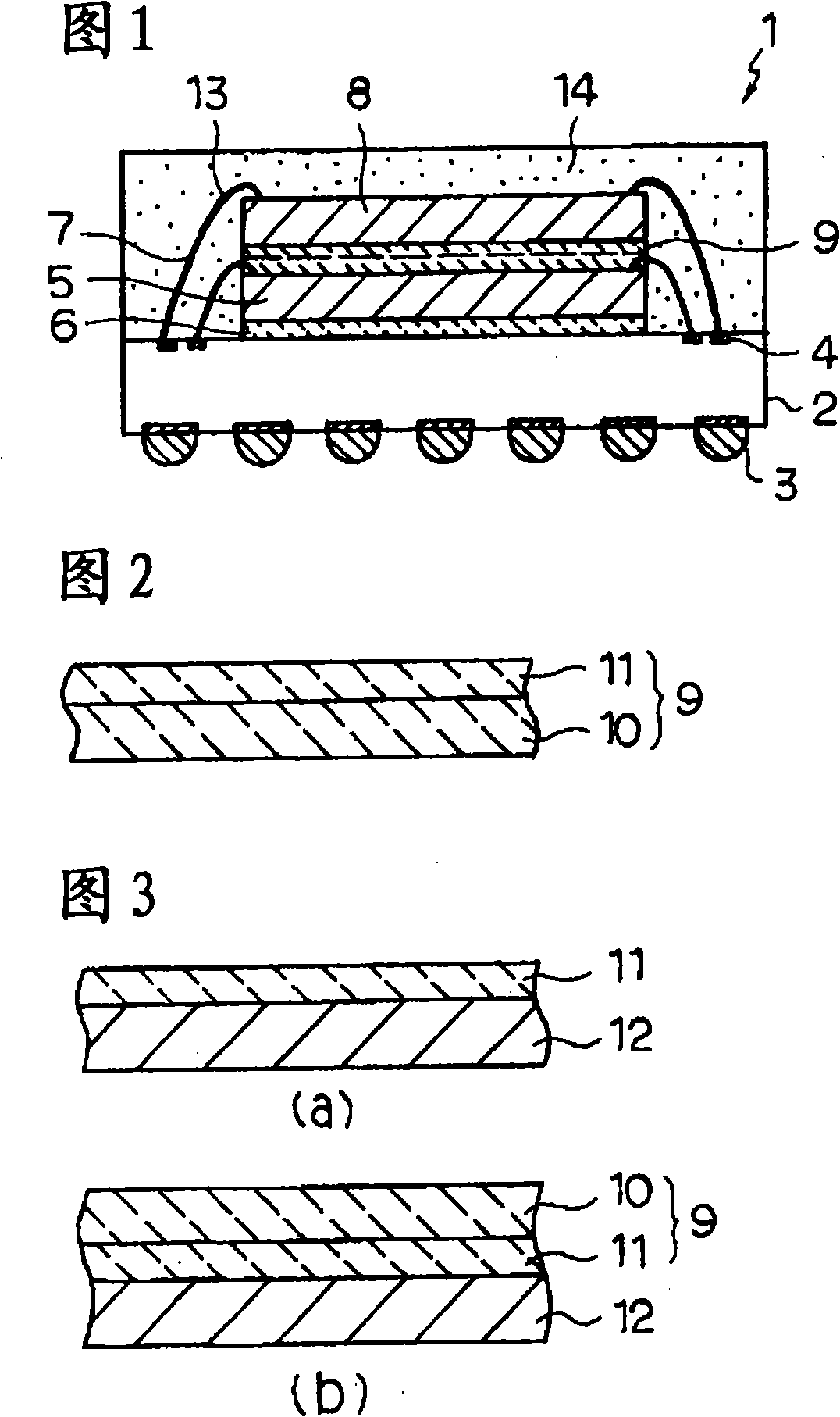
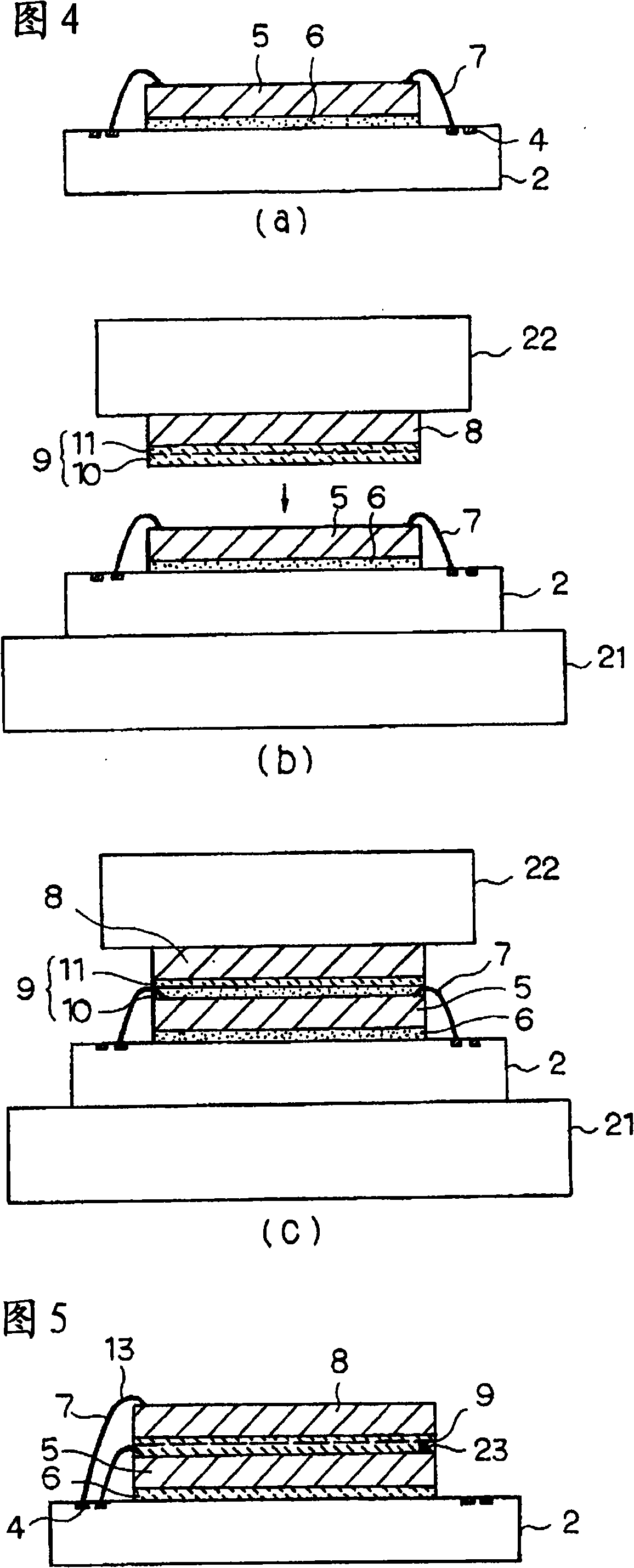
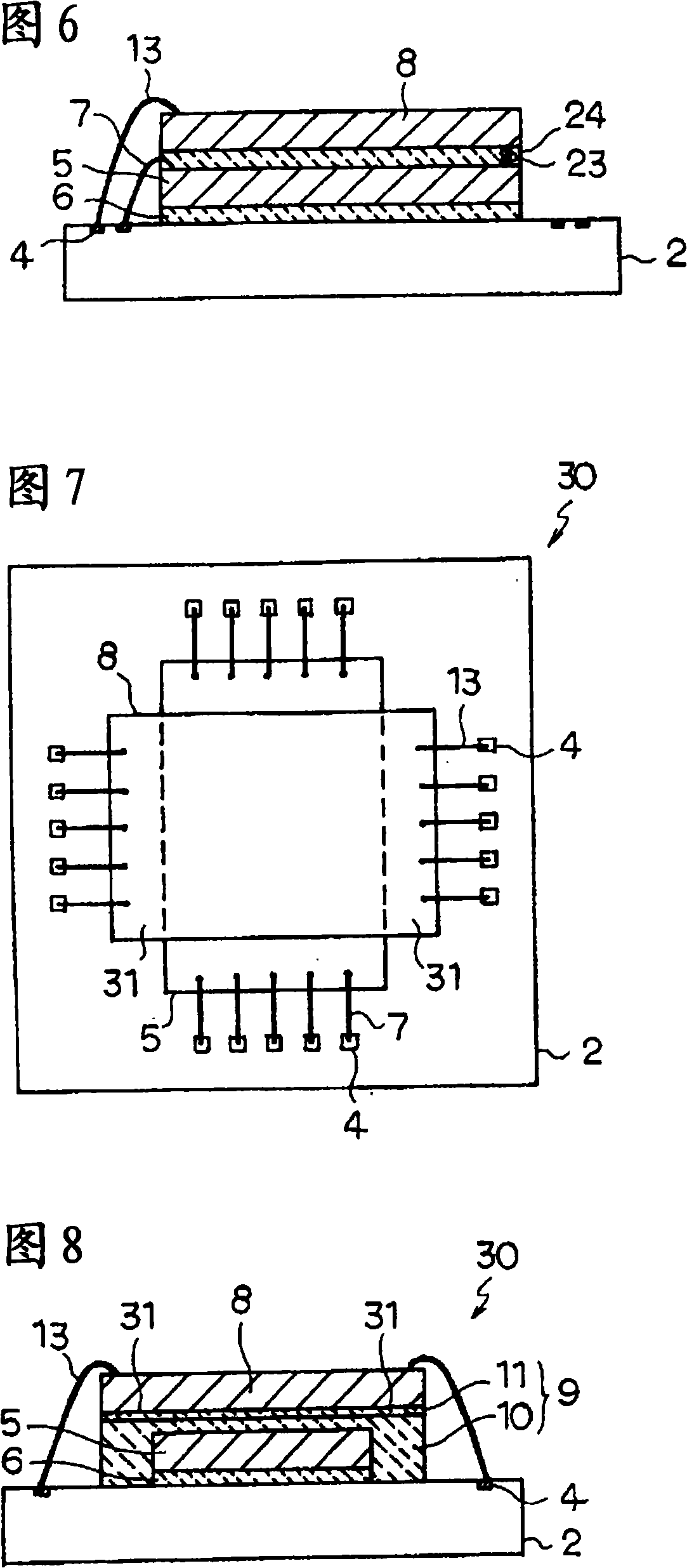
The invention provides a semiconductor device, which is characterized by including a substrate with an electrode section; a first semiconductor component, which has a first electrode solder pad connected on the electrode section by a first bonding lead, and is adhered onto the substrate; and a second semiconductor component, which has a second electrode solder pad connected on the electrode section by a second bonding lead, and is adhered onto the first semiconductor component by an adhesive agent layer which has a two-layer structured formed by the same material and having different elastic rates.
Description
Semiconductor device technical field The present invention relates to a semiconductor device in which a plurality of semiconductor elements are stacked. Background technique In recent years, a stacked multi-chip package in which a plurality of semiconductor elements (semiconductor chips) are stacked and packaged in a single package has been put into practical use in order to achieve miniaturization and high-density packaging of semiconductor devices. In such a stacked multi-chip package, a plurality of semiconductor elements are sequentially stacked on a mounting substrate such as a circuit board through an adhesive such as a die-bonding material, and the electrodes of each semiconductor element are electrically connected by bonding wires. Electrode parts such as pads and circuit boards. In addition, by encapsulating such a laminated structure with a sealing resin, a laminated multi-chip package is constituted. However, in the stacked multi-chip package described above,...
Claims
Login to View More Application Information
Patent Timeline
 Patent Type & AuthorityApplications(China)
IPC IPC(8): H01L25/00H01L23/28H01L23/00H01L25/065
CPCH01L2224/92247H01L2224/32225H01L2224/48227H01L2224/73265H01L2224/32145H01L2225/06562H01L24/73H01L2924/00012H01L2924/00
Inventor芳村淳小牟田直幸沼田英夫
Owner키오시아가부시키가이샤