Method and system for realizing high-resolution sub-pixel imaging technique

An imaging system and sub-pixel technology, applied in radio wave measurement systems, optical components, electromagnetic wave re-radiation, etc., to achieve low-cost effects

Inactive Publication Date: 2008-11-05
SHANGHAI INST OF TECHNICAL PHYSICS - CHINESE ACAD OF SCI
View PDF0 Cites 3 Cited by
  • Summary
  • Abstract
  • Description
  • Claims
  • Application Information

AI Technical Summary

Problems solved by technology

[0003] The purpose of the present invention is to provide a new type of sub-pixel imaging system and method based on an ordinary area array CMOS detector imaging instrument, so as to solve the problem that the current sub-pixel imaging needs to customize a special arrangement of detectors

Method used


Image

  • Method and system for realizing high-resolution sub-pixel imaging technique
  • Method and system for realizing high-resolution sub-pixel imaging technique
  • Method and system for realizing high-resolution sub-pixel imaging technique

Examples


Embodiment Construction

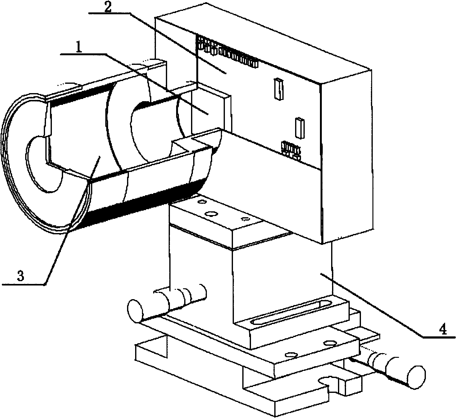
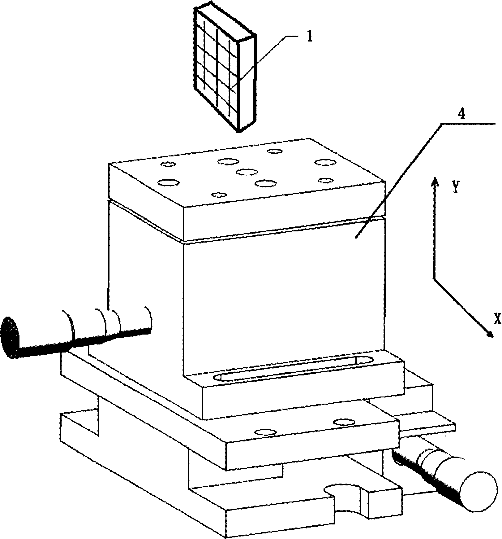
[0020] Attached below Figure 1 ~ Figure 3 The specific implementation of the device for realizing sub-pixel detection of the present invention is described in detail:

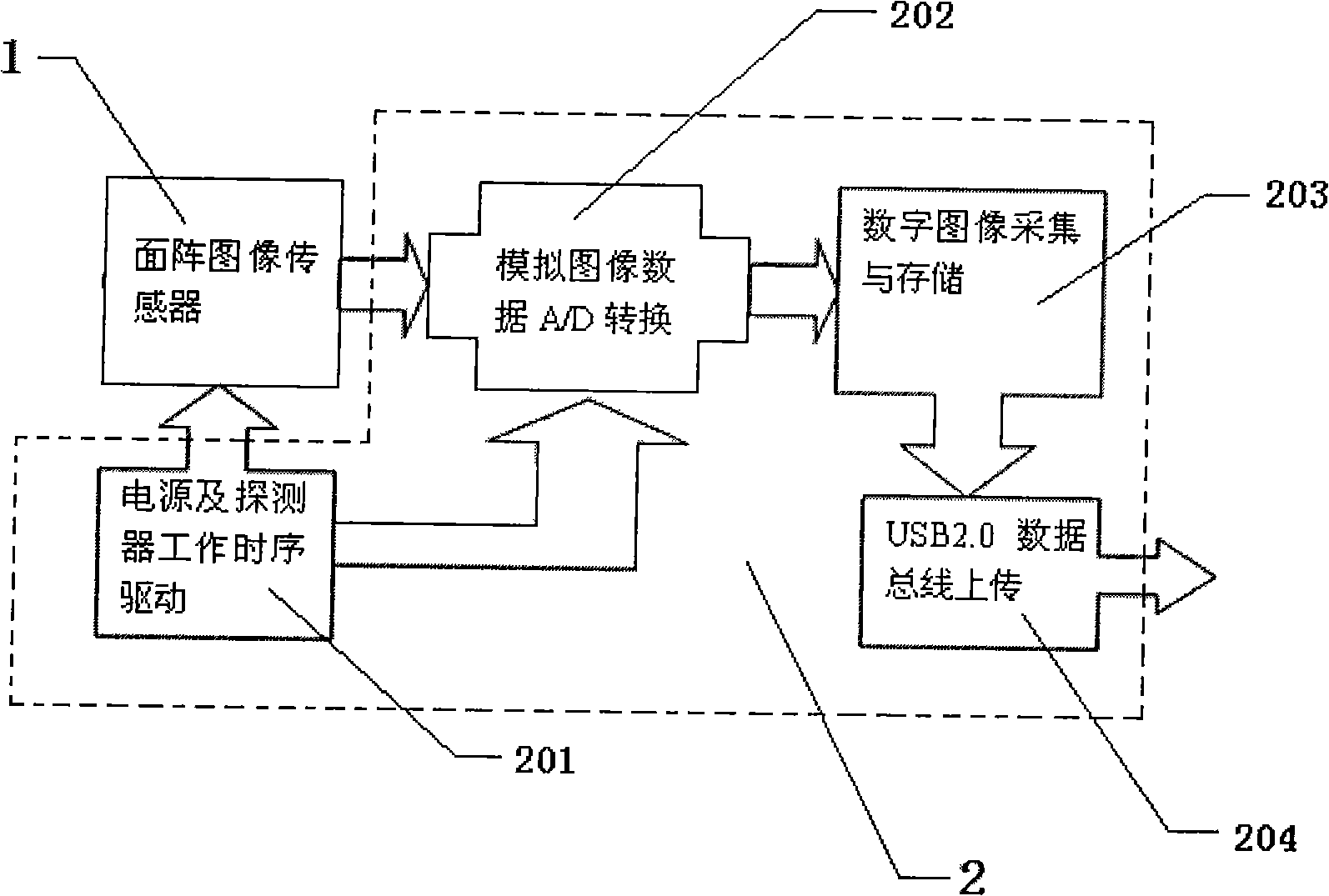
[0021] as attached figure 1 Shown, the said common area array CMOS detector 1 of the present invention is to adopt the CMOS area array detector that the pixel arrangement mode is arranged at square equidistant, specifically adopts the STAR250 type black and white area array CMOS detector of Cypress Company; Said The optical lens 3 adopts a Kenko 500mm fixed-focus lens; the two-dimensional translation precision optical adjustment device 4 adopts the combination of the TSM25G-1S ultra-precision translation stage and the TSMV5-1A precision lifting platform of Beijing Zhuoli Hanguang Instrument Co., Ltd. Said area array CMOS detector drive and data acquisition board 2 is composed of power supply and detector work timing drive module 201, analog image data A / D conversion module 202, digital image acquisition and s...


PUM


Abstract

The present invention discloses a method for realizing a high resolution sub-pixel imaging technique and a system thereof, wherein the system comprises the following components: a common planar array CMOS detector; a planar array CMOS detector driving and data collecting board; an optical lens and a two-dimensional parallel-moving precise optical adjusting bracket. The sub-pixel detection of the imaging system can be realized through executing a two-dimensional parallel moving to the common planar array CMOS detector to research the sub-pixel detection technique. The advantage of the invention is that a flexible two-dimensional parallel mechanical structure is used for facilitating the imaging system of common planar array CMOS detector executes sub-pixel detection. The customizing of a special detector can be avoided. Furthermore the effect of sub-pixel detection technique with different registration precision of image can be researched flexibly through controlling the two-dimensional parallel moving displacement amount thereby realizing that the sub-pixel technique research which is more appropriate to engineering is executed in a short period and under a low cost.

Description

technical field [0001] The present invention relates to sub-pixel imaging technology, specifically a method and system for realizing high-resolution sub-pixel imaging technology, which is used for high-resolution imaging of objects. Background technique [0002] Using sub-pixel technology for super-resolution image reconstruction is an effective means to improve the spatial resolution of images, and it is also an important branch in the field of image processing. In recent years, many domestic scholars are also studying sub-pixel detection technology, but the research mainly focuses on In algorithm research, this kind of research has little correlation with actual instrument research, so it has great limitations and limited guiding significance. However, for actual experiments, detectors with special arrangements need to be customized, and the production cost is very high and the cycle time is relatively long. Contents of the invention [0003] The purpose of the present ...

Claims


Application Information

Patent Timeline
Patent Type & Authority Applications(China)
IPC IPC(8): G02B27/58G01S17/89
Inventor 陈博洋罗勇陈凡胜孙胜利陈桂林
Owner SHANGHAI INST OF TECHNICAL PHYSICS - CHINESE ACAD OF SCI
Why Eureka
Try Eureka