Printing plate for intaglio offset and manufacturing method thereof, methods for manufacturing substrate and display apparatus

A manufacturing method and printing plate technology, which can be applied in the directions of printed circuit manufacturing, printing device, offset printing, etc., can solve the problems of the plane shape of the ink film 121 without good reproducibility and transfer, and it is difficult to apply and manufacture TFT substrates, etc.

Inactive Publication Date: 2008-11-12
NEC LCD TECH CORP
View PDF4 Cites 10 Cited by
  • Summary
  • Abstract
  • Description
  • Claims
  • Application Information

AI Technical Summary

Problems solved by technology

Therefore, there is a problem that the method is difficult to apply to the case of manufacturing TFT substrates in which various patterns need to be formed
[0031] Also, there is a problem that when the ink film 121 embedded in the recess 110b is transferred to the blanket 131, the planar shape and / or size of the ink film 121 are not transferred in a good reproducible manner.
Therefore, in the case where the intaglio offset printing method is carried out using the removal plate or printing plate disclosed in this publication, it is apparent that the intaglio offset printing method disclosed in Japanese Patent No. 3730002 (see FIG. 3 ) has the same problem as

Method used


Image

  • Printing plate for intaglio offset and manufacturing method thereof, methods for manufacturing substrate and display apparatus
  • Printing plate for intaglio offset and manufacturing method thereof, methods for manufacturing substrate and display apparatus
  • Printing plate for intaglio offset and manufacturing method thereof, methods for manufacturing substrate and display apparatus

Examples


no. 1 example

[0117] Structure of the print edition

[0118] Image 6 A schematic structural view of a printing plate 10 for reversed relief offset printing according to a first embodiment of the present invention is shown in .

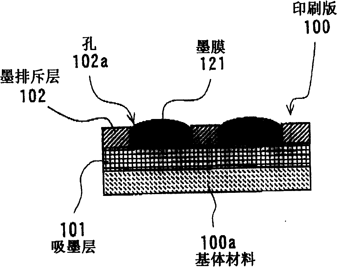
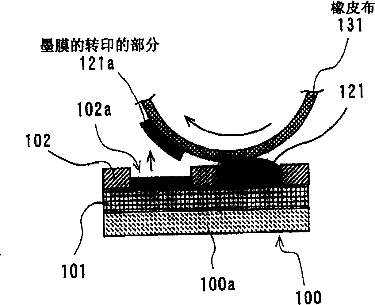
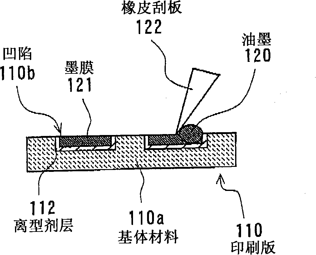
[0119] Such as Image 6 As shown in , the printing plate 10 according to the first embodiment includes a plate-shaped base material 10a having recesses 11a and 11b on its surface, and ink repellent layers 12a and 12a respectively formed on the inner surfaces of the recesses 11a and 11b. 12b. The entire inner surfaces of the recesses 11a and 11b are covered with ink repellent layers 12a and 12b, respectively. As a result, depressions 13a and 13b are formed on the surface of base material 10a. The depression 13a is defined by the concave portion 11a and the ink repelling layer 12a. The depression 13b is defined by the concave portion 11b and the ink repelling layer 12b. The portion of the plate 10 other than the recesses 13 a and 13 b is the non-recessed portio...

no. 2 example

[0193] Figure 13B is a schematic partial cross-sectional view of a printing plate 10A according to a second embodiment of the present invention.

[0194] The printing plate 10A according to the second embodiment is covered with a pattern-formed Cr film 41A except that the surface of the plate-shaped base material 10a (that is, the surface other than the concave portion 14) in the region other than the concave portions 11a and 11b is covered with a patterned Cr film 41A. Structurally the same as the printing plate 10 according to the first embodiment. Therefore, by giving Figures 12A to 12C and Figures 13A to 13BThe same or corresponding parts in 10 are attached with the same reference numerals used in the first embodiment, and the explanation of the same structure is omitted.

[0195] With the printing plate 10A of the second embodiment, the surface of the non-recessed portion 14 of the base material 10a is covered with the patterned Cr film 41A, so the ink-absorbing surfa...

no. 3 example

[0212] Figure 16 is a partial cross-sectional view of a printing plate 10B according to a third embodiment of the present invention.

[0213] Except that the flat surface 10aa of the plate-like base material 10a (that is, the flat surface of the non-recessed portion 14) in the region other than the concave portions 11a and 11b is roughened by minute protrusions and dimples, according to the second embodiment The printing plate 10B is identical in structure to the printing plate 10 according to the first embodiment. Therefore, by giving Figures 14A to 14C , Figures 15A to 15C with Figure 16 The same or corresponding parts in 10 are attached with the same reference numerals used in the first embodiment, and the explanation of the same structure is omitted.

[0214] With the printing plate 10A of the third embodiment, since the surface 10aa of the non-recessed portion 14 becomes rough, the ink affinity of the non-recessed portion 14 is higher than that of the surface of t...


PUM


Abstract

A printing plate for reversed relief offset printing ensures the prevention of the internal omission of a desired pattern without increasing the depths of depressions of the plate. The printing plate comprises a base material having depressions and a non-depressed part on a surface thereof, and ink repellent layers that cover inner surfaces of the depressions, respectively. The depressions of the base material whose inner surfaces are respectively covered with the ink repellent layers have a plan shape that defines a desired pattern. The non-depressed part of the base material is formed in such a way that a part of an ink film corresponding to the non-depressed part can be transferred to the printing plate in a process of reversed relief offset printing. The parts of the ink film corresponding to the depressions are not transferred to the printing plate due to the repelling action of the ink repellent layers.

Description

technical field [0001] The present invention relates to a printing plate and a method of manufacturing the same, a method of manufacturing a substrate for a display device, and a method of manufacturing a display device. More specifically, the present invention relates to a printing plate for reversed relief offset printing, wherein the depressed inner surfaces of the printing plate are respectively covered with an ink repellent layer; a method of manufacturing the printing plate; a A method of manufacturing a display device including a minute pattern, such as a liquid crystal display (LCD) device, an organic electroluminescence (EL) display device, a plasma display device; and a method of manufacturing a substrate for such a display device as described above. Background technique [0002] In recent years, LCD devices have been widely used as high-resolution display devices. The LCD device includes a substrate on which a switching element such as a thin film diode (TFT) is ...

Claims


Application Information

Patent Timeline
Patent Type & Authority Applications(China)
IPC IPC(8): B41M1/00B41N1/00B41C1/00
CPCG02B5/201H05K2203/0108B41N1/06H05K2203/0534H05K3/1275G02F1/133516B41N1/20G02B5/223B41C1/00H05K2203/0143B41M1/10B41N1/22B41N1/12H05K2203/1173
Inventor 高松秀明
Owner NEC LCD TECH CORP
Why Eureka
Try Eureka