An organic material transfer printing method in an organic light-emitting display

A light-emitting display and organic material technology, applied in the direction of copying/marking methods, printing, electric solid devices, etc., can solve the problems of abnormal OLED products, metal mask deformation, high defective rate, etc., and achieve small thermal expansion coefficient and small deformation , the effect of high processing precision

Active Publication Date: 2015-07-01
KUNSHAN VISIONOX DISPLAY TECH
View PDF7 Cites 5 Cited by
  • Summary
  • Abstract
  • Description
  • Claims
  • Application Information

AI Technical Summary

Problems solved by technology

[0004] For this reason, the technical problem to be solved by the present invention is that the existing methods of manufacturing organic light-emitting displays by evaporation are only suitable for manufacturing small-sized OLED screens, and in the production of some OLEDs with larger sizes or larger substrates, The metal mask plate is prone to deformation, resulting in abnormalities in the produced OLED products, high defective rate, and serious waste

Method used


Image

  • An organic material transfer printing method in an organic light-emitting display
  • An organic material transfer printing method in an organic light-emitting display

Examples


Embodiment 1

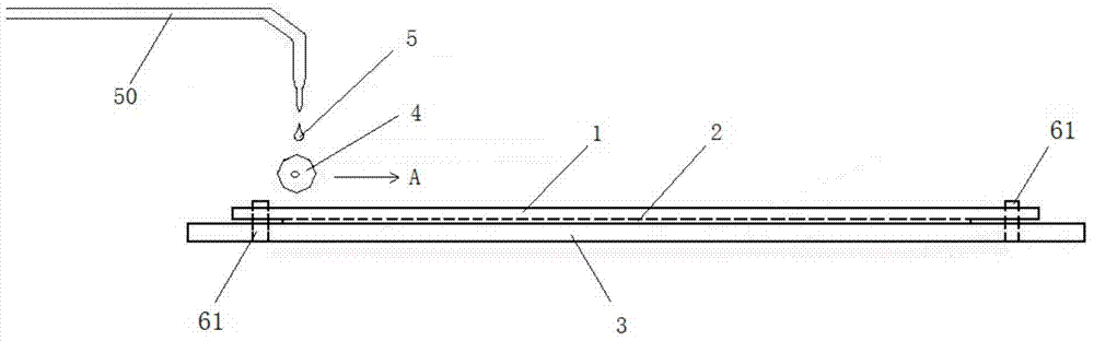
[0032] see figure 1 It is a transfer printing method of an organic material on an organic light-emitting display disclosed in the present invention, which is used to produce a monochrome device structure, and the organic material 5 is a hole injection layer, a hole transport layer, a light-emitting layer, an electron transport layer, An electron injection layer, comprising the steps of:

[0033] Step 1 - positioning the substrate 2 for transferring the organic material 5 on the fixed platform 3, the substrate 2 being a glass substrate;

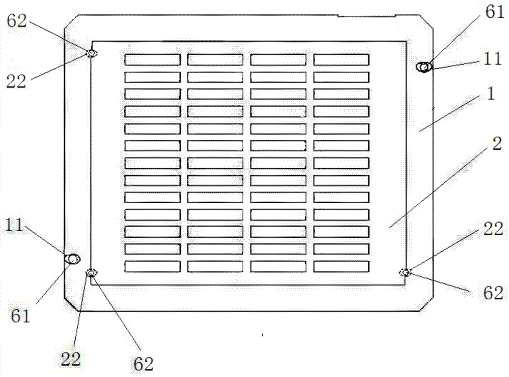
[0034] Step 2 - According to the final formed structure of the substrate 2, design a film mask 1 with a hollow figure shape, attach it to the substrate 2, and position the film mask 1 on the fixed platform 3;

[0035] Step 3 - dripping the liquid organic material 5 onto the roller 4 through the conduit 50;

[0036] Step 4 - lower the height of the roller 4 so that it has a suitable height between it and the substrate 2, through the circumfer...

Embodiment 2

[0047] The transfer printing method of the organic material on the organic light-emitting display of this embodiment is used to produce a multi-color or color device structure, and the organic material 5 is a hole injection layer, a hole transport layer, a light-emitting layer, an electron transport layer, an electron The injection layer, wherein the multi-color light-emitting layer is a combination of multiple monochromatic light-emitting materials, and the light-emitting layer of the color device includes red light material, yellow light material, and blue light material respectively, and the color is formed through the combination of RGB.

[0048] Above-mentioned transfer printing method comprises the following steps:

[0049] Step 1 - positioning the substrate 2 for transferring the organic material 5 on the fixed platform 3, the substrate 2 being a glass substrate;

[0050] Step 2 - According to the final formed structure of the substrate 2, design a film mask 1 with a ho...

other Embodiment approach

[0057] In other implementation manners, the thin film mask 1 can be selected from thin films such as stainless steel thin films and ferroelectric thin films.

[0058] In addition, the liquid organic material 5 in step 3 can also be made in other ways, such as heating the organic material 5 to the melting point to form a molten organic material 5 .


PUM


Abstract

An organic material transfer printing method in an organic light-emitting display is disclosed. The method includes following steps of: 1) positioning a substrate on a fixed platform; 2) tightly attaching a film mask onto the substrate and positioning the film mask on the fixed platform; 3) evenly arranging a liquid organic material onto the wheel surface of an idler wheel; 4) subjecting the organic material to transfer printing onto the substrate by rotation and movement of the idler wheel; 5) removing water in the organic material subjected to transfer printing on the substrate to turn the organic material into a solid state; and 6) when a monochromatic device structure is produced, repeating the step 3) to the step 5) so that the organic material is subjected to transfer printing on the substrate layer by layer; and when a multicolor or color device structure is produced, changing the film mask according to an organic material to be subjected to transfer printing and subjecting the organic material to transfer printing to the substrate layer by layer. The film mask used in the method can improve processing precision of the organic light-emitting display. When being used for production of large-size OLED screens and large-size substrates, the method can ensure OLED screens to be free of abnormity and ensure product quality.

Description

technical field [0001] The invention relates to the technical field of organic light emitting display manufacturing, in particular to an organic material transfer printing method on an organic light emitting display. Background technique [0002] In the production process of organic light-emitting display (OLED, Organic Light-Emitting Diode screen body), the evaporation method is generally used at present. During evaporation, a mask (MASK) with a certain graphic shape needs to be produced first. The traditional MASK It is made of stainless steel, and the MASK is fixed on the support frame by stretching technology and welding technology to form a whole metal MASK, and then evaporated in the graphics surrounded by the metal MASK. [0003] For example, Chinese patent document CN102021517 discloses a screen-type evaporation source and evaporation method in the OLED preparation process, which includes a vacuum chamber and a heat source placed in the vacuum chamber from top to bot...

Claims


Application Information

Patent Timeline
Patent Type & Authority Applications(China)
IPC IPC(8): B41M5/00H01L51/56
Inventor 尤沛升
Owner KUNSHAN VISIONOX DISPLAY TECH
Why Eureka
Try Eureka