

Photocuring resin composition, dry film, and print circuit board
A technology of photocurable resin and composition, applied in secondary processing of printed circuits, optics, optomechanical equipment, etc., can solve problems such as defects, and achieve the effects of reduced halogen gas generation, excellent concealment, and low halogen content
- Summary
- Abstract
- Description
- Claims
- Application Information
AI Technical Summary
Problems solved by technology
Method used
Image

Examples
Embodiment 1~7 and comparative example 1~2
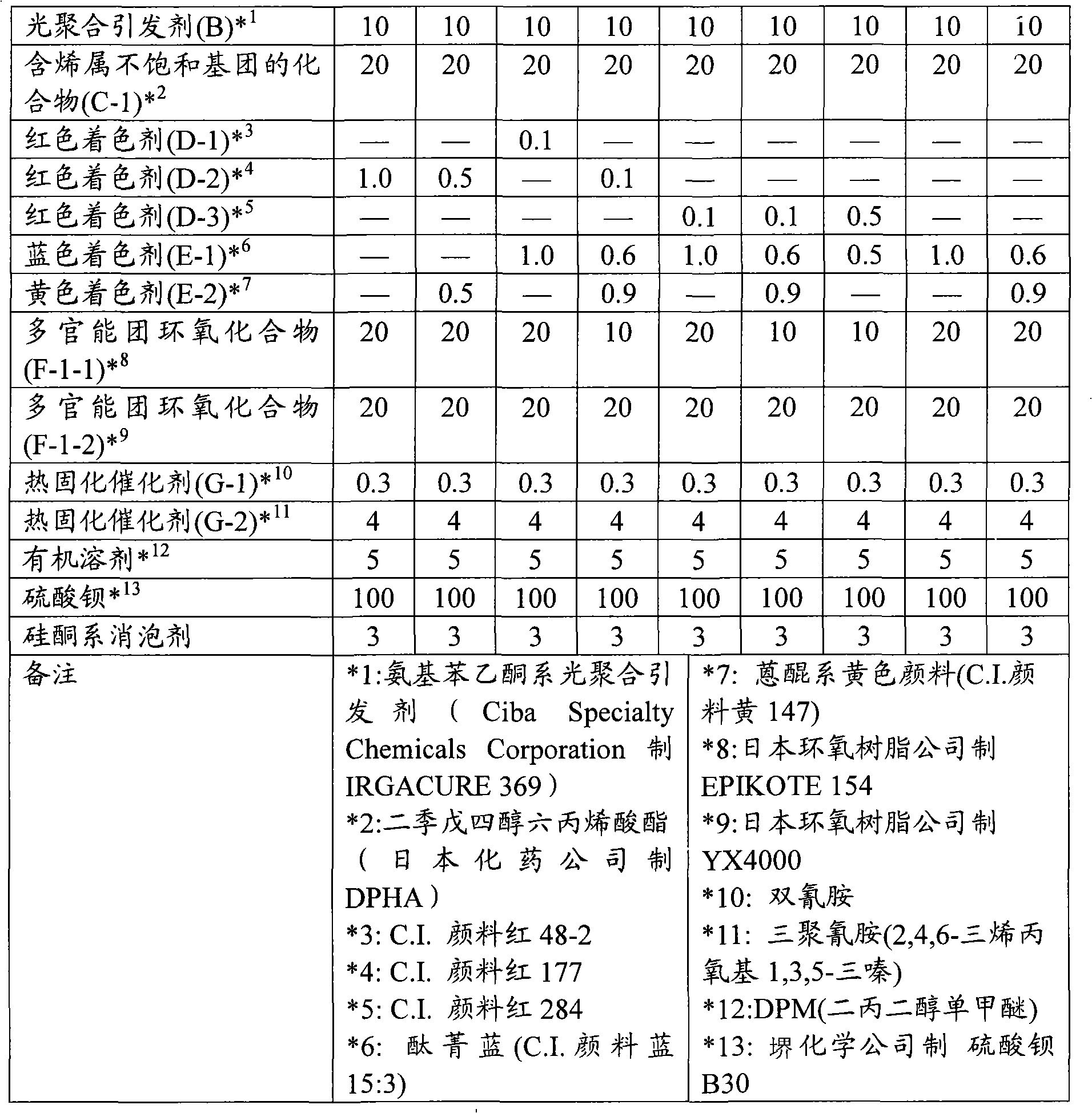
[0116] The varnish (A-1) obtained in the synthesis of the carboxylic acid-containing resin and the components shown in Table 1 were kneaded at the compounding ratios shown in Table 1 using a three-roll mill to obtain a photocurable resin composition.
[0117] Table 1
[0118]
[0119]
[0120] About the photocurable resin composition of Examples 1-7 and Comparative Examples 1-2, performance and characteristic were evaluated according to the following evaluation criteria. The results are shown in Table 2.
[0121] Performance evaluation:
[0122]
[0123] The circuit pattern substrate with a copper thickness of 35 μm is polished and ground, washed with water, dried, and then the photocurable resin composition of Examples 1-7 and Comparative Examples 1-2 is coated on the entire surface by the screen printing method. Dry in a circulating drying oven for 60 minutes. After drying, use an exposure device equipped with a metal halide lamp to expose through a step exposure ...
PUM
 Abstract
Description
Claims
Application Information