
Shift buffer capable of reducing frequency coupling effect and shift buffer unit

A shift register and frequency signal technology, applied in static memory, digital memory information, instruments, etc., can solve problems such as poor pull-down effect, not being pulled down in time, and slow rising speed of waveform

Active Publication Date: 2008-11-12
AU OPTRONICS CORP
View PDF1 Cites 31 Cited by
  • Summary
  • Abstract
  • Description
  • Claims
  • Application Information

AI Technical Summary

Problems solved by technology

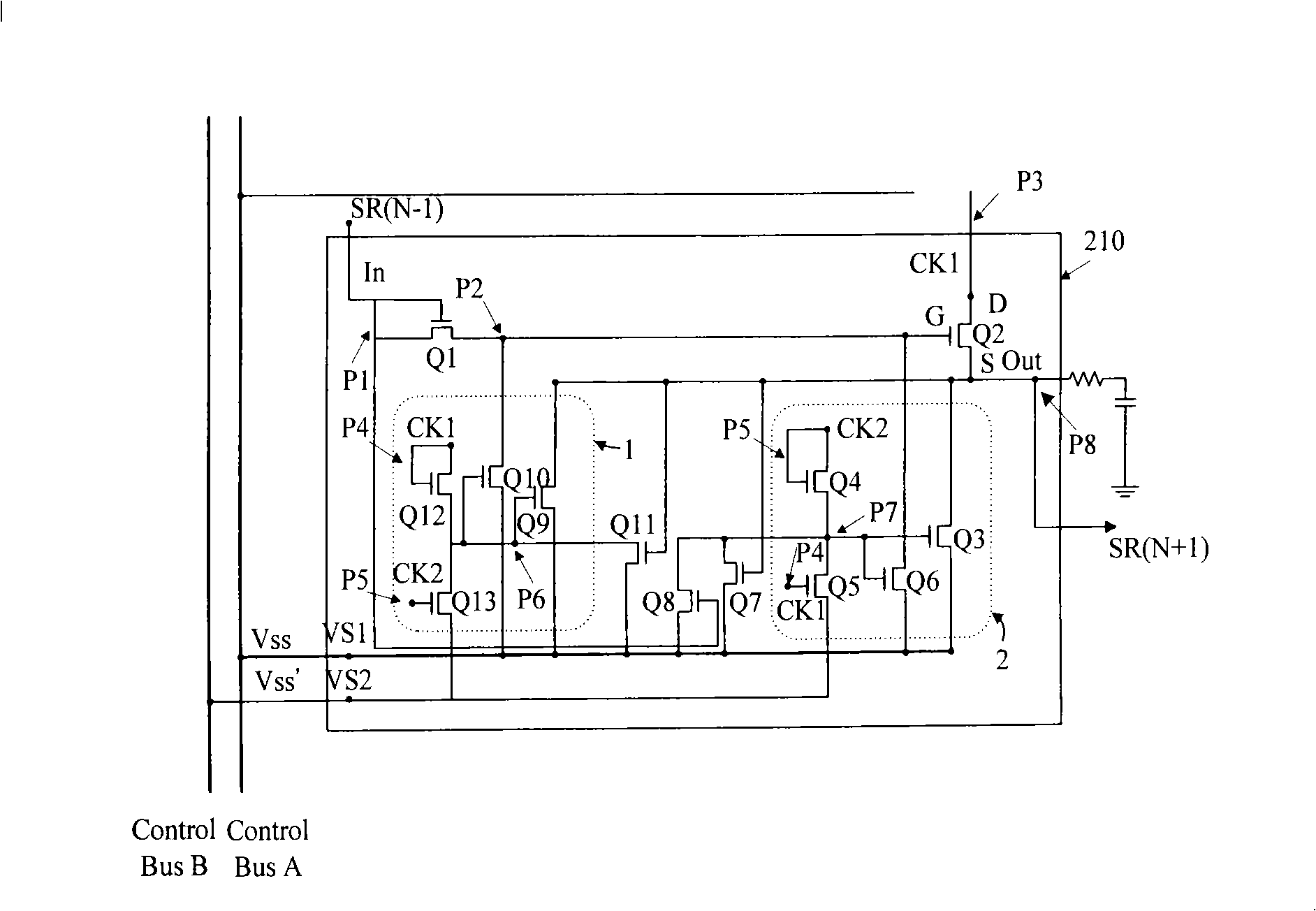
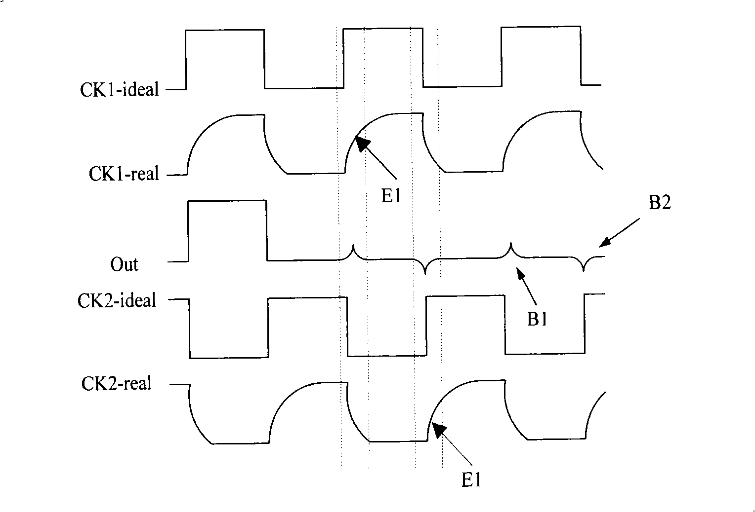
like Figure 1A As shown, it is a circuit diagram of the Nth-stage shift register 210 disclosed in US Patent No. 7310402B2, which includes a boost transistor Q2 and pull-down modules 1 and 2 that both use a first frequency signal (CK1) as shown in the figure The ideal first frequency signal (CK1-ideal) waveform, but actually in operation, it is susceptible to a capacitance (Cgd) coupling effect ( Coupling Effect) impact, resulting in such as Figure 1B The shown waveform of the actual first frequency signal (CK1-real) rises slowly (such as the edge E1 of the curve), resulting in several periodic rising points B1 in the output waveform (Out) of the gate pulse signal; at the same time ,because Figure 1A The pull-down modules 1 and 2 are also driven by the delay of the first frequency signal (CK1), which jointly causes the level of the output node or input node (such as P2) of the boost module to not be pulled down in time, so that the pull-down effect is not good
In addition, although the pull-down module 2 uses the ideal second frequency signal (CK2-ideal), the actual second frequency signal (CK2-real) may also have the same coupling effect problem as the first frequency signal, so as Figure 1B The output waveform (Out) of the gate pulse signal shown also has several periodic downward sudden rise points B2

Method used


Image

  • Shift buffer capable of reducing frequency coupling effect and shift buffer unit
  • Shift buffer capable of reducing frequency coupling effect and shift buffer unit
  • Shift buffer capable of reducing frequency coupling effect and shift buffer unit

Examples


Embodiment Construction

[0066] The technical content of the present invention will be described in detail below with reference to illustrations.

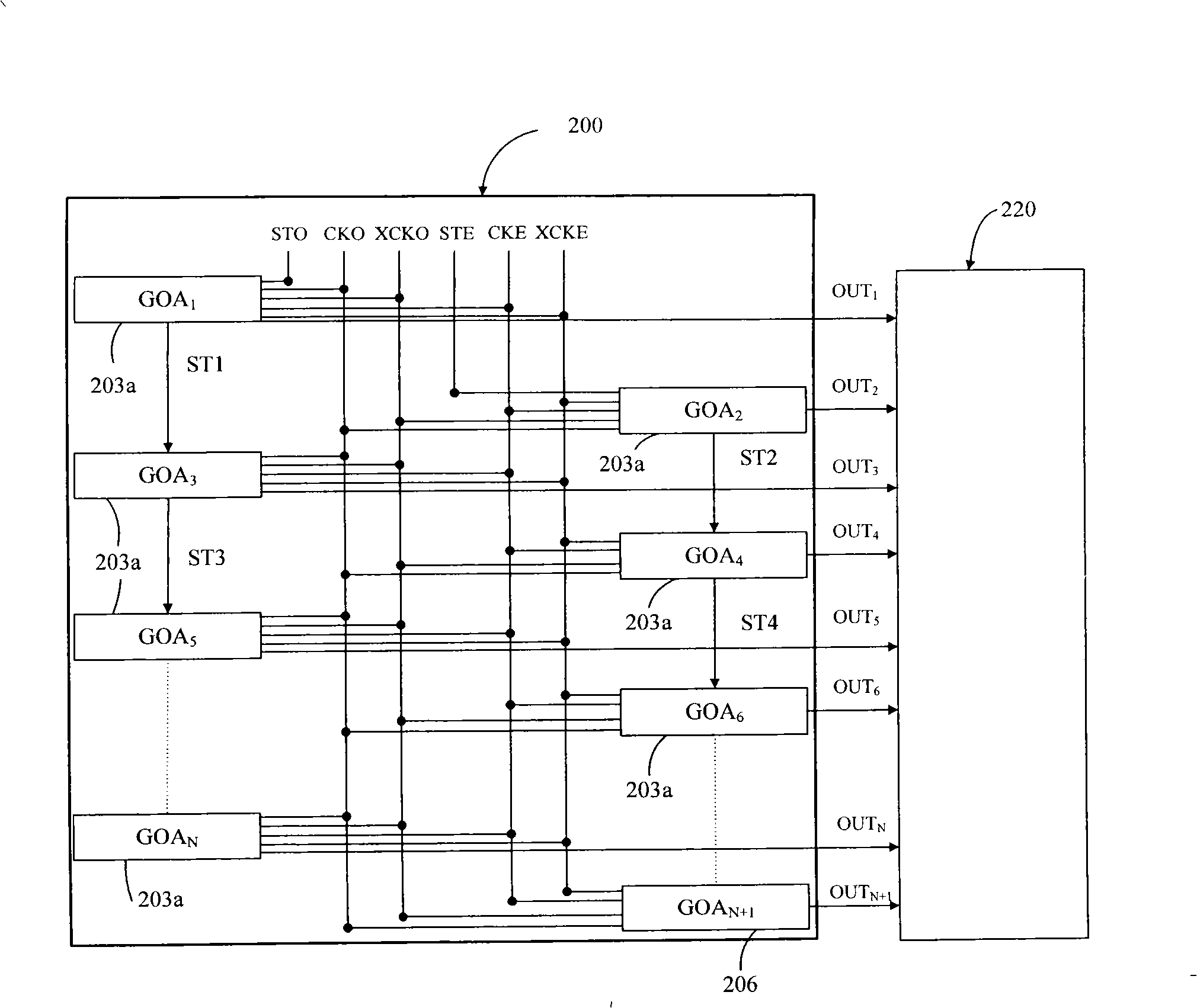
[0067] Please see first figure 2 , is a shift register 200 according to the first preferred embodiment of the present invention, comprising a plurality of serially connected odd-numbered stage shift register units (GOA1, GOA3-GOAN) 203a and a plurality of serially connected even-numbered stages The shift register unit (GOA1, GOA3-GOAN) 203a is characterized in that the odd-numbered and even-numbered shift register units 203a output gate pulse signals sequentially through several gate lines or scan lines ( Out1~OutN+1) to respectively trigger the gates (Gate) of each thin film transistor (TFT) constituting the array pixel (Pixel) 220 in a liquid crystal display (LCD) panel, to store the information transmitted from the relevant data line (not shown) Grayscale data. Among the series-connected odd-stage shift register units (GOA1, GOA3-GOAN) 203a, except t...


PUM


Abstract

The invention discloses a displacement buffer which can reduce a frequency coupling effect and a displacement buffer unit; wherein every level of the displacement buffer unit comprises at least a lifting driving module, a lifting module, at least a pull-down module and a pull down driving module; wherein, before a first frequency signal waveform or a second frequency signal waveform used by the lifting module forms an ascending edge, the pull-down driving module opens the conduction of the pull-down module for a particular period according to a first periodic signal; and / or before the first frequency signal waveform or the second frequency signal waveform used by the lifting module forms an descending edge, the pull-down driving module closes the conduction of the pull-down module for a particular period according to a second periodic signal; therefore, when the coupling effect of the frequency signal appears at that time, the pull-down module has enough ability to resist so as to improve the output waveform of the displacement buffer unit.

Description

technical field [0001] The invention relates to a shift register and a shift register unit, in particular to a shift register and a shift register unit capable of reducing frequency coupling effects. Background technique [0002] A conventional liquid crystal display (LCD) utilizes a driving module (Driving Circuit) to control the grayscale signals of a plurality of pixels (Pixels) on the panel of the liquid crystal display. The drive module includes a gate driver (GateDriver) electrically connected to several scan lines (or gate lines) to respectively output a gate pulse signal (Gate PulseSignal) to each corresponding pixel, and a source driver (Source Driver) is electrically connected to several data lines (or source lines) to respectively transmit the data signal (Data Signal) to each corresponding pixel, and the intersection of each scanning line and each data line is also connected to a corresponding The polarity terminals of the active element of the pixel (such as th...

Claims


Application Information

Patent Timeline
IPC IPC(8): G11C19/00G11C19/28G09G3/36
Inventor 蔡宗廷赖明升陈勇志刘柏源
Owner AU OPTRONICS CORP
Learn More