Semiconductor element mounting board and optical transmission module

a technology of semiconductor elements and mounting boards, applied in the direction of optical elements, semiconductor lasers, instruments, etc., can solve the problems of increasing the number of components to be mounted and the mounting area, reducing the size of the transceiver and its production cost, and creating unnecessary gain (peaking), so as to reduce the output waveform of an optical modulator, reduce the small signal reflection coefficient, and suppress the peaking of small signal passage characteristics

Active Publication Date: 2008-07-15
LUMENTUM JAPAN INC
View PDF9 Cites 7 Cited by
  • Summary
  • Abstract
  • Description
  • Claims
  • Application Information

AI Technical Summary

Benefits of technology

[0016]According to the invention, it is possible to acquire the construction that can simultaneously suppress peaking in small signal passage characteristics (S21) for improving the output waveform of an optical modulator in an optical transmission module of a single power source driving system and can reduce a small signal reflection coefficient (S11), and can accomplish an optical transmission module most suitable for an optical transfer transceiver for high speed signals (for example, 10 Gbit / s).

Problems solved by technology

Therefore, the number of components to be mounted and the mounting area increase, and this circuit construction is extremely disadvantageous for reducing the size of the transceiver and its production cost.
According to this circuit form, however, a very small inductance of the bonding wire added creates an unnecessary gain (peaking) in small signal passage characteristics of the optical modulator.
As a result, it is difficult to acquire satisfactory output waveform quality even when an attempt is made to improve the characteristics by shortening the length of the bonding wire to the ground electrode within the range in which packaging is possible.

Method used


Image

  • Semiconductor element mounting board and optical transmission module
  • Semiconductor element mounting board and optical transmission module
  • Semiconductor element mounting board and optical transmission module

Examples


embodiment 1

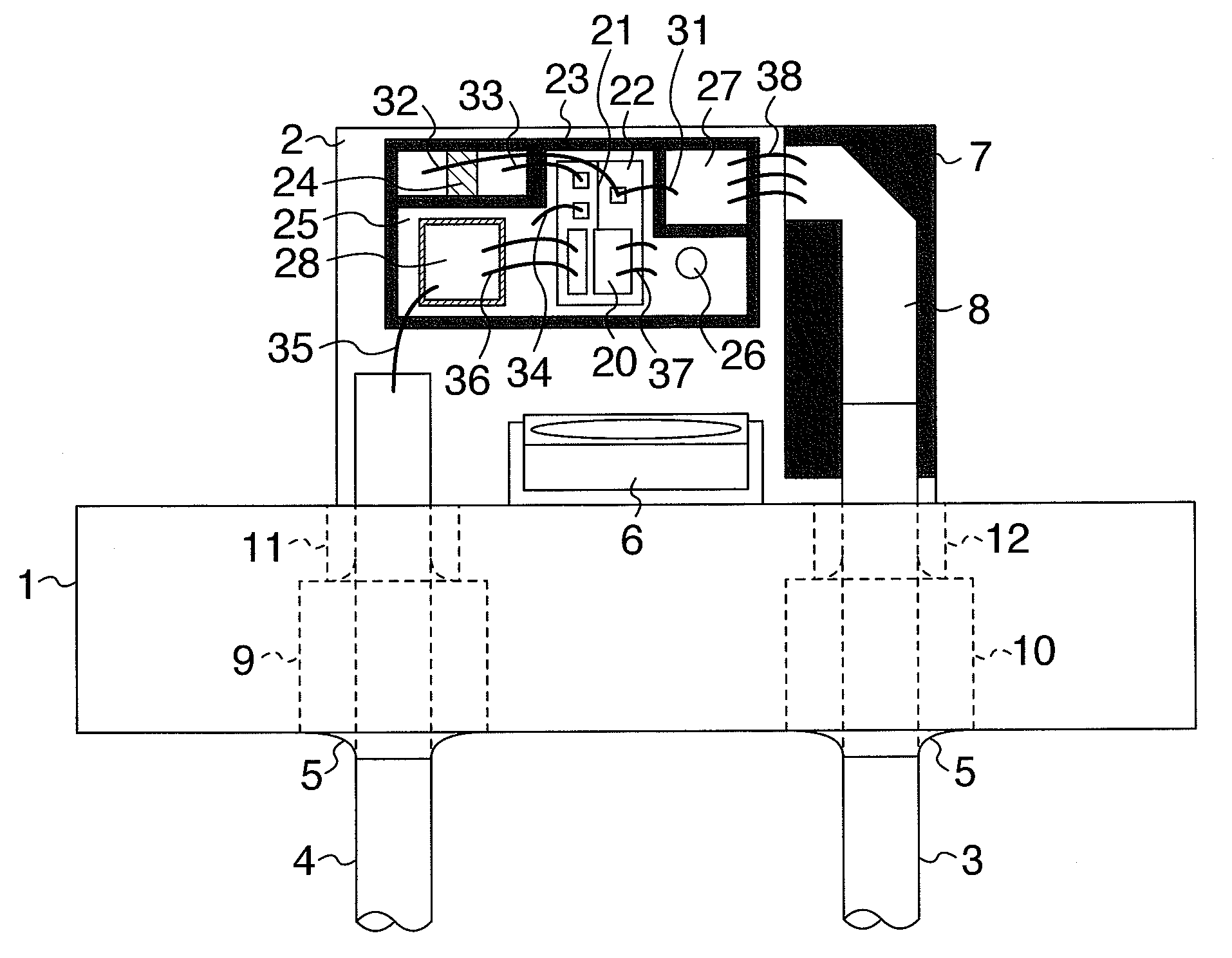
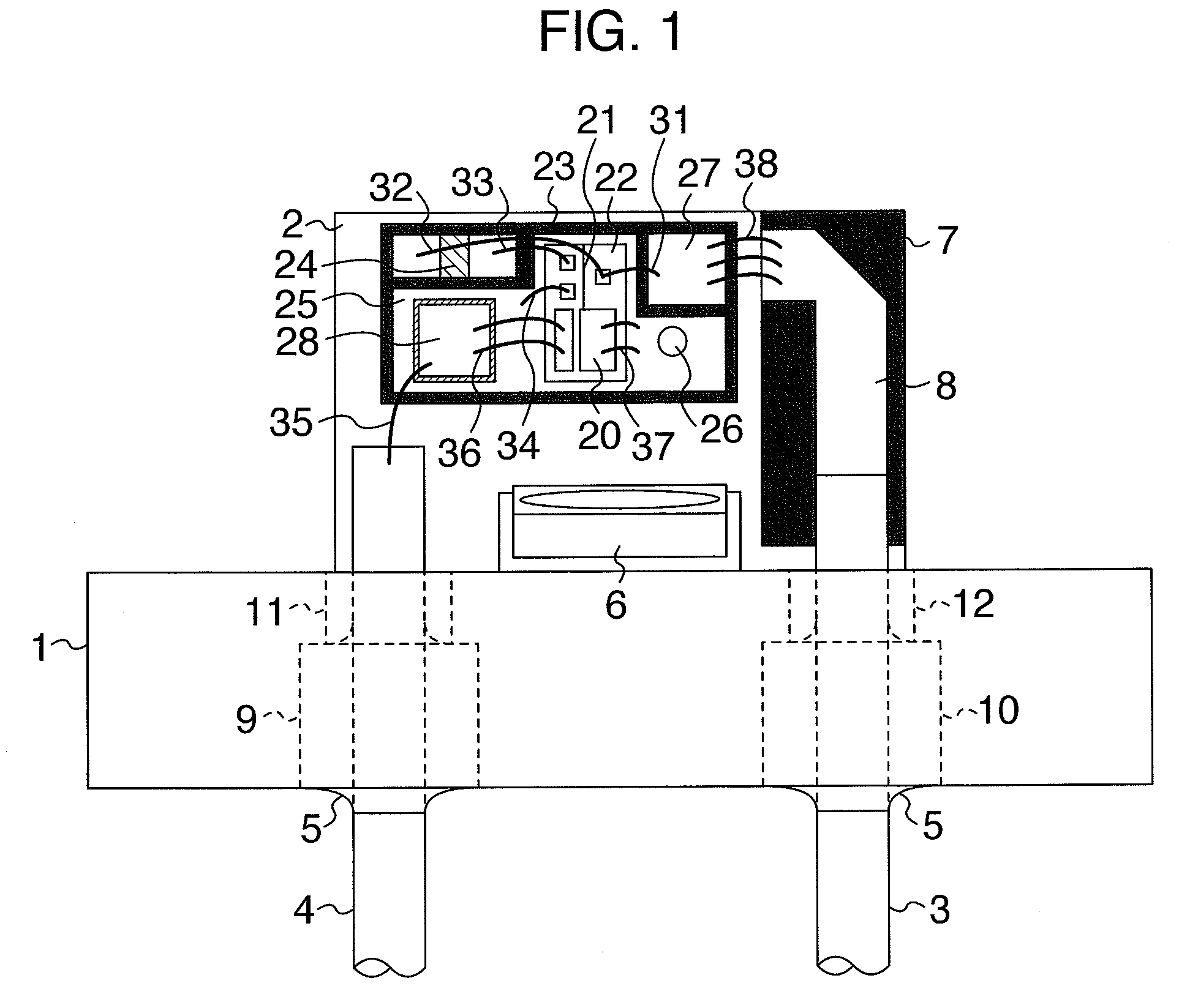
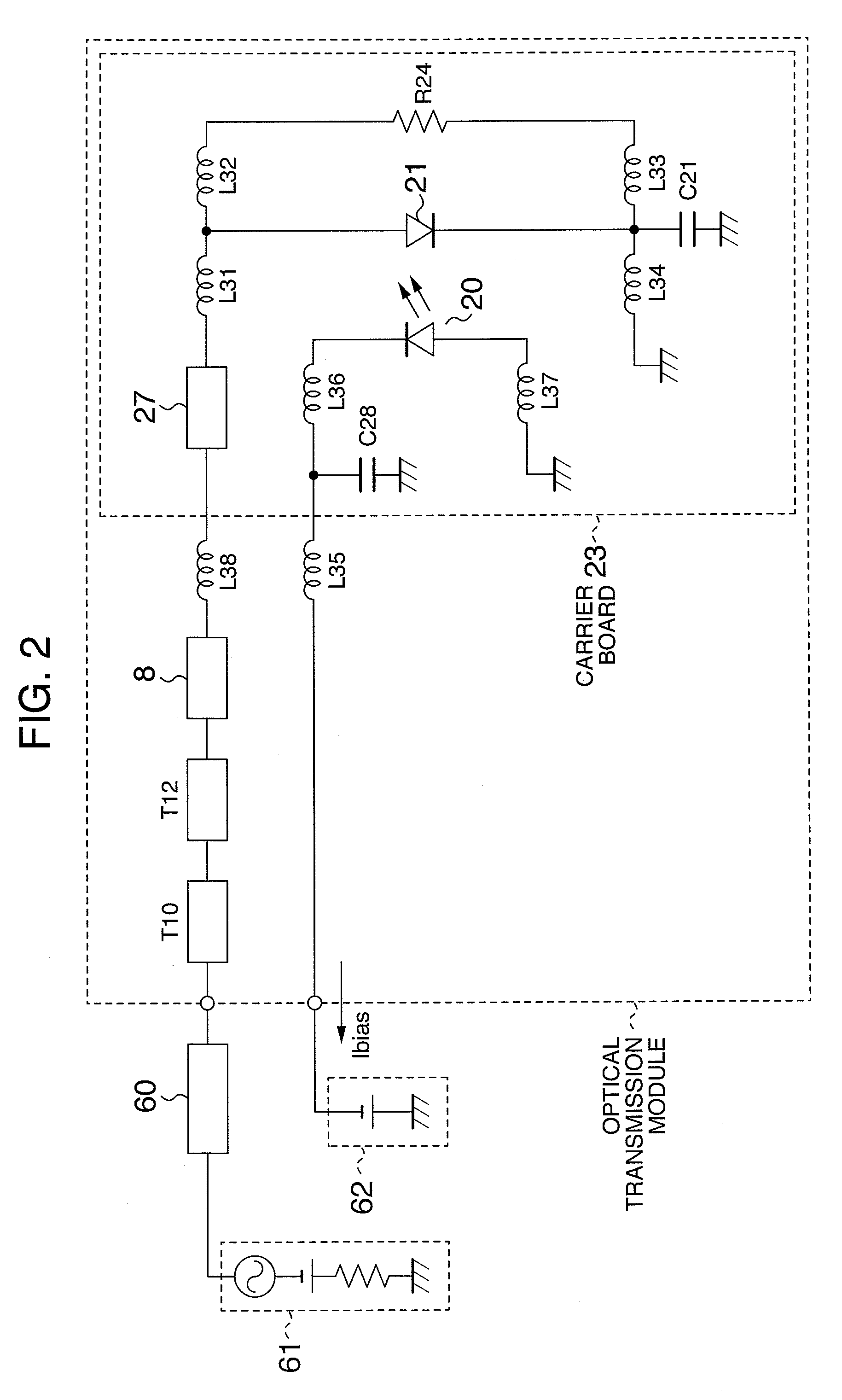
[0042]The first embodiment of the invention will be explained with reference to FIGS. 1 through 3 and FIGS. 9 through 13.

[0043]FIG. 1 is a structural view that shows main portions of an optical transmission module according to this embodiment, FIG. 2 is a main circuit diagram of the optical transmission module, and FIG. 3 is a detailed view of a carrier board portion for mounting optical semiconductor elements. FIG. 9 is a graph showing the relation between a frequency and electric-optical small signal passage characteristic S21 of the optical transmission module, FIG. 10 shows an optical output waveform of the optical transmission module, and FIGS. 11 through 13 are graphs respectively showing excessive gain characteristics, 3 dB band characteristics and input reflection characteristics S11 of the optical transmission module when inductance of a bonding wire to be connected to an optical modulator element is changed.

[0044]First, the construction of the optical transmission module w...

embodiment 2

[0082]The second embodiment of the invention will be explained with reference to FIGS. 4 to 6 and FIGS. 19 to 22.

[0083]FIG. 4 is a structural view that shows main portions of an optical transmission module according to this embodiment. FIG. 5 is a main circuit diagram of the optical transmission module. FIG. 6 is a detailed view of a carrier board portion. FIG. 19 is a graph that shows input reflection characteristics S11 of this embodiment. FIG. 20 is a graph that shows small signal passage characteristics S21.

[0084]As shown in FIGS. 4 and 6, the main differences from the embodiment 1 reside in that the arrangement of the anode and cathode of the surface electrodes of the semiconductor chip 122 is reversed to the right and left and that the input transfer line 127 is extended to a portion below the optical modulator element 21. Independent back electrodes are disposed below the optical modulator element 121 and the semiconductor laser diode element 120 on the back of the semiconduc...

embodiment 3

[0091]The third embodiment of the invention will be explained with reference to FIGS. 7 and 8.

[0092]FIG. 7 is a structural view that shows main portions of an optical transmission module according to this embodiment. FIG. 8 is a main circuit diagram of the optical transmission module. The main difference from the second embodiment described above resides in that the optical modulator element 21 is driven by differential electric modulation signals.

[0093]The construction of the optical transmission module will be first explained with reference to FIG. 7. The optical transmission module uses a CAN type package casing as its casing. Reference numeral 1 denotes a metal stem and reference numeral 2 denotes a metal seat for mounting a main portion. Circular cylindrical lead pins 3 and 4 are provided to the metal stem 1 through through-holes 209 and 210 and are fixed by sealing glass 5. Relay boards 205 and 207 and a carrier board 223 are mounted onto the metal seat 2. A transfer line 206 ...


PUM

PropertyMeasurementUnit
impedanceaaaaaaaaaa
diameteraaaaaaaaaa
resistanceaaaaaaaaaa

Abstract

An optical transmission module of the invention uses a semiconductor chip forming an optical modulator integrated laser on a semi-insulating semiconductor board. An input transfer line and an anode electrode of an optical modulator element are connected by a first bonding wire. The anode electrode of the optical modulator element and one of the ends of a terminal resistor element are connected by a second bonding wire. A cathode electrode of the optical modulator element and the other end of the terminal resistor element are connected by a third bonding wire. The cathode electrode of the optical modulator element and a ground electrode are connected by a fourth bonding wire. A joint portion between the first bonding wire and the input transfer line is arranged on an opposite side to a joint portion between the fourth bonding wire and the ground electrode while interposing the semiconductor chip between them.

Description

INCORPORATION BY REFERENCE[0001]The present application claims priority from Japanese application JP2006-115147 filed on Apr. 19, 2006, the content of which is hereby incorporated by reference into this application.BACKGROUND OF THE INVENTION[0002]This invention relates to an optical transmission module for optical communication, and particularly to an optical transmission module used for a transmission portion of an optical transceiver having a high transfer rate (10 Gbit / s, for example).[0003]An optical transmission module using a semiconductor laser is one of the key devices of transceivers for optical fiber transfer. An operation speed of optical transmission modules has been improved with recent popularization of broadband networks and optical transmission modules having a transfer rate of up to 10 Gbit / s have now been used widely. The optical transmission modules suitable for this application are strongly required to possess small size and low cost and to achieve high transmis...

Claims


Application Information

Patent Timeline
Patent Type & Authority Patents(United States)
IPC IPC(8): G02B6/12G02F1/015H01S5/022
CPCH01S5/02248H01L24/49H01L2224/48227H01S5/0208H01S5/02212H01S5/02276H01S5/0265H01S5/0422H01S5/0427H01S5/06226H01S5/0683H01L2224/49H01L2224/48091H01L2224/48137H01L2924/3011H01L2924/30107H01L2224/49175H01L2224/49111H01L2924/00014H01L2924/00H01L2924/12042H01L2224/45014H01L24/48H01S5/02325H01S5/02345H01L2224/45099H01L2224/45015H01L2924/207H01L2924/206
Inventor KAGAYA, OSAMU
Owner LUMENTUM JAPAN INC
Why Eureka
Try Eureka