

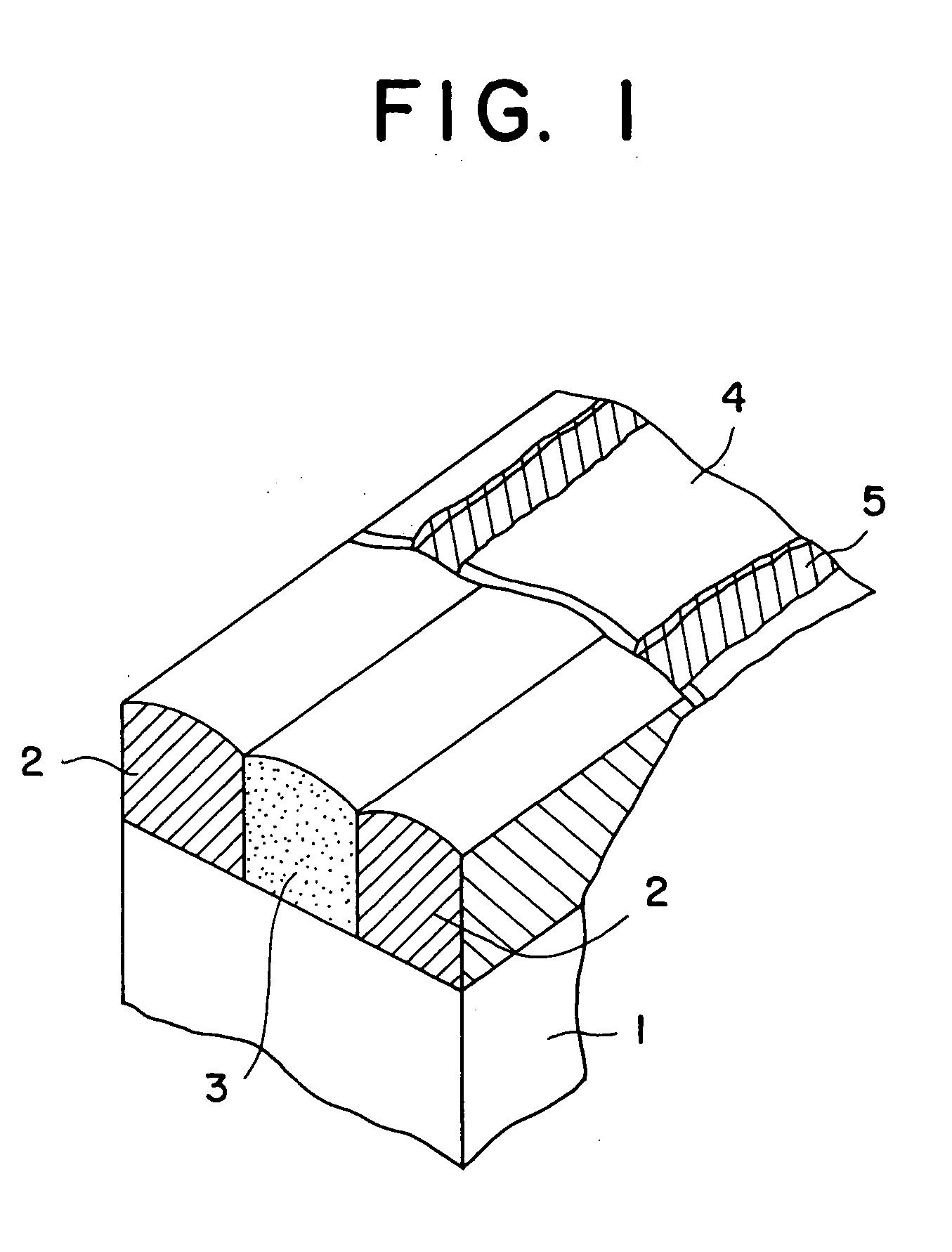
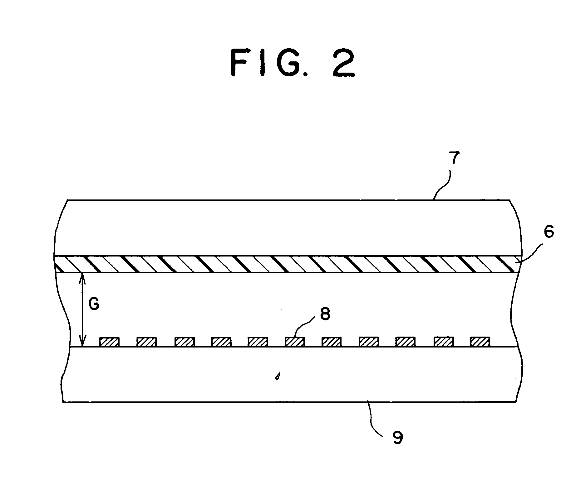
Method of forming metal back-attached fluorescent surface and image display unit
a technology of fluorescent surface and image display unit, which is applied in the manufacture of tubes with screens, electric discharge tubes/lamps, and applications of luminescent coatings, etc. it can solve the problems of high cost and large-scale devices, electron emission elements of cathode sections and phosphor screens of anode sections destructed or damaged, and the momentary concentration of energy can be avoided. , the reflection effect of the metal back layer is hardly decreased
- Summary
- Abstract
- Description
- Claims
- Application Information
AI Technical Summary
Benefits of technology
Problems solved by technology
Method used
Image

Examples
example 2
[0047] After the Al film was formed on the phosphor screen in the same way as in Example 1, a treating solution consisting of 5% of NaOH, 1% of Na-based water glass and the remainder of water was applied to the Al film and baked in the same way as in Example 1.
[0048] By the application of the solution and baking as described above, the Al film of the applied portion was oxidized and became a highly resistant layer having a surface resistivity on the order of 10.sup.10.OMEGA. / . And, this high resistant Al oxide layer having a stripe pattern was formed on the conductive Al film. It was confirmed by observing through a microscope that there was no curl at the ends (boundary portions with the Al oxide layer) of the Al film.
[0049] Then, a panel having the metal back-attached phosphor screen was used as a face plate to fabricate an FED in the same way as in Example 1.
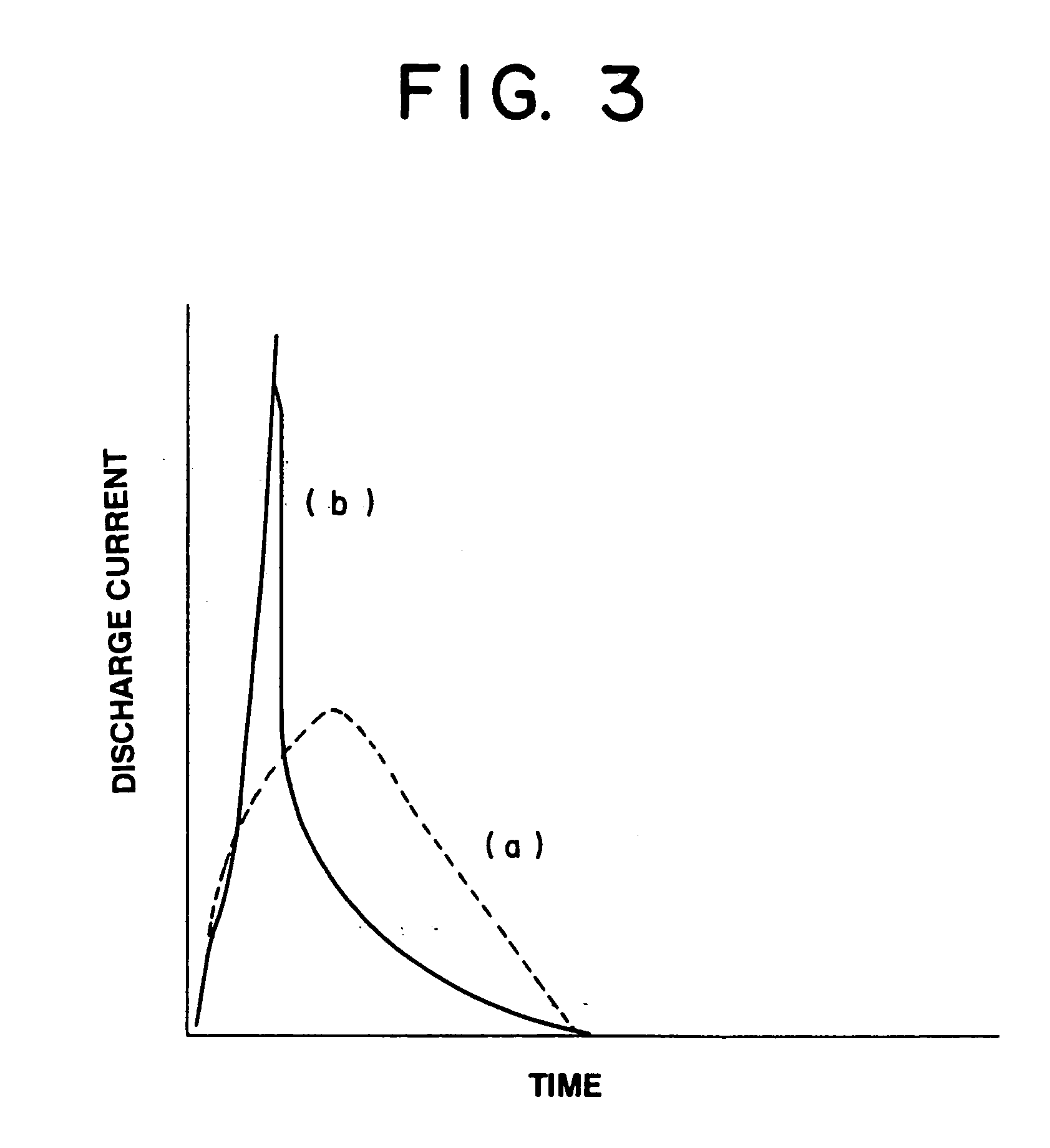
[0050] The FED obtained in Example 2 was measured for evaluation of its withstand pressure characteristic by a common proce...
example 3
[0051] After the Al film was formed on the phosphor screen in the same way as in Example 1, an ink having the prescribed composition was printed on an area of the Al film on the light absorption layer, and baking was conducted at 450.degree. C. for 30 minutes.
[0052] After the treatment, the Al film was measured its surface resistance to find that a portion where the ink was not printed had a surface resistivity of approximately 1.OMEGA. / , while the printed portion had a surface resistivity on the order of 10.sup.5.OMEGA. / , and the coated portions of the Al film were dissolved / removed by ink printing and baking.
[0053] Then, a panel having such a metal back-attached phosphor screen was used as a face plate to fabricate an FED in the same way as in Example 1.
[0054] The FED produced in Example 3 was measured for evaluation of its withstand pressure characteristic by a common procedure. The maximum voltage (maximum withstand voltage) was improved to 15 kV higher than that in Example 1. A...
PUM
| Property | Measurement | Unit |
|---|---|---|
| pH | aaaaa | aaaaa |
| pH | aaaaa | aaaaa |
| voltage | aaaaa | aaaaa |
Abstract
Description
Claims
Application Information