Semiconductor device and method of forming the same
一种半导体、器件的技术,应用在半导体器件、半导体/固态器件制造、半导体/固态器件零部件等方向,能够解决晶体管锁定噪声容限退化、不足以保持晶体管稳定运行等问题
- Summary
- Abstract
- Description
- Claims
- Application Information
AI Technical Summary
Problems solved by technology
Method used
Image

Examples
Embodiment Construction
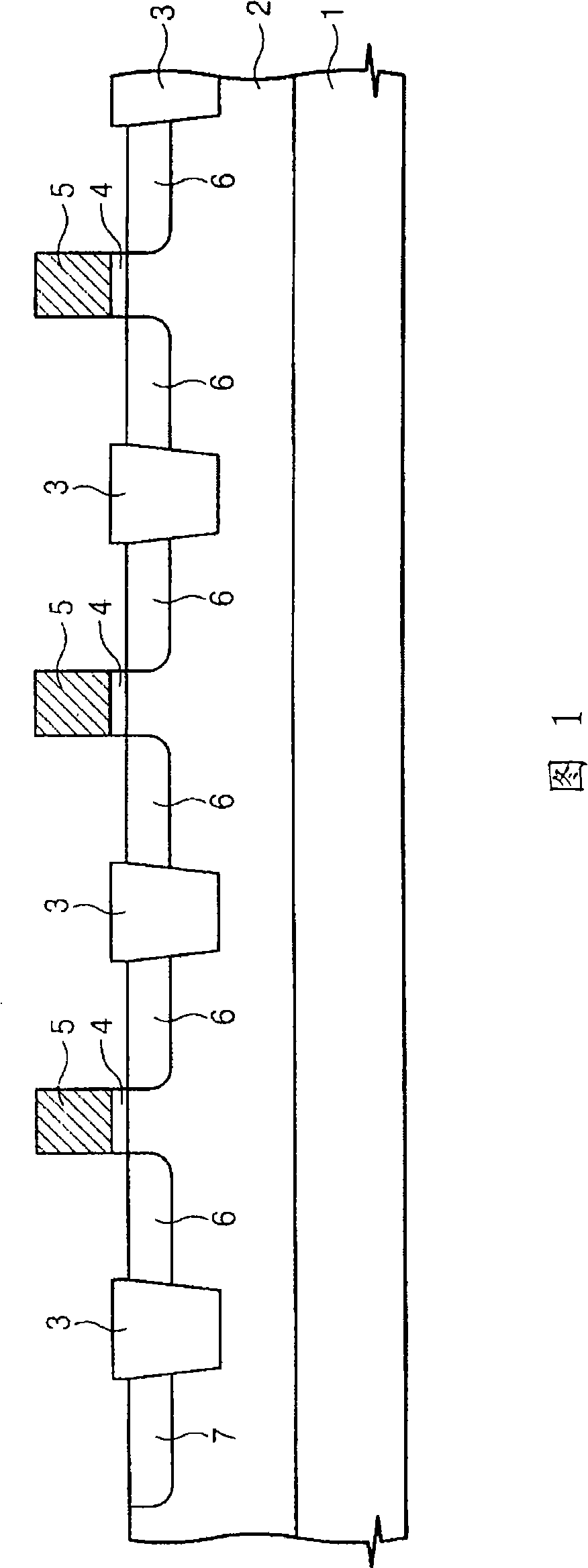
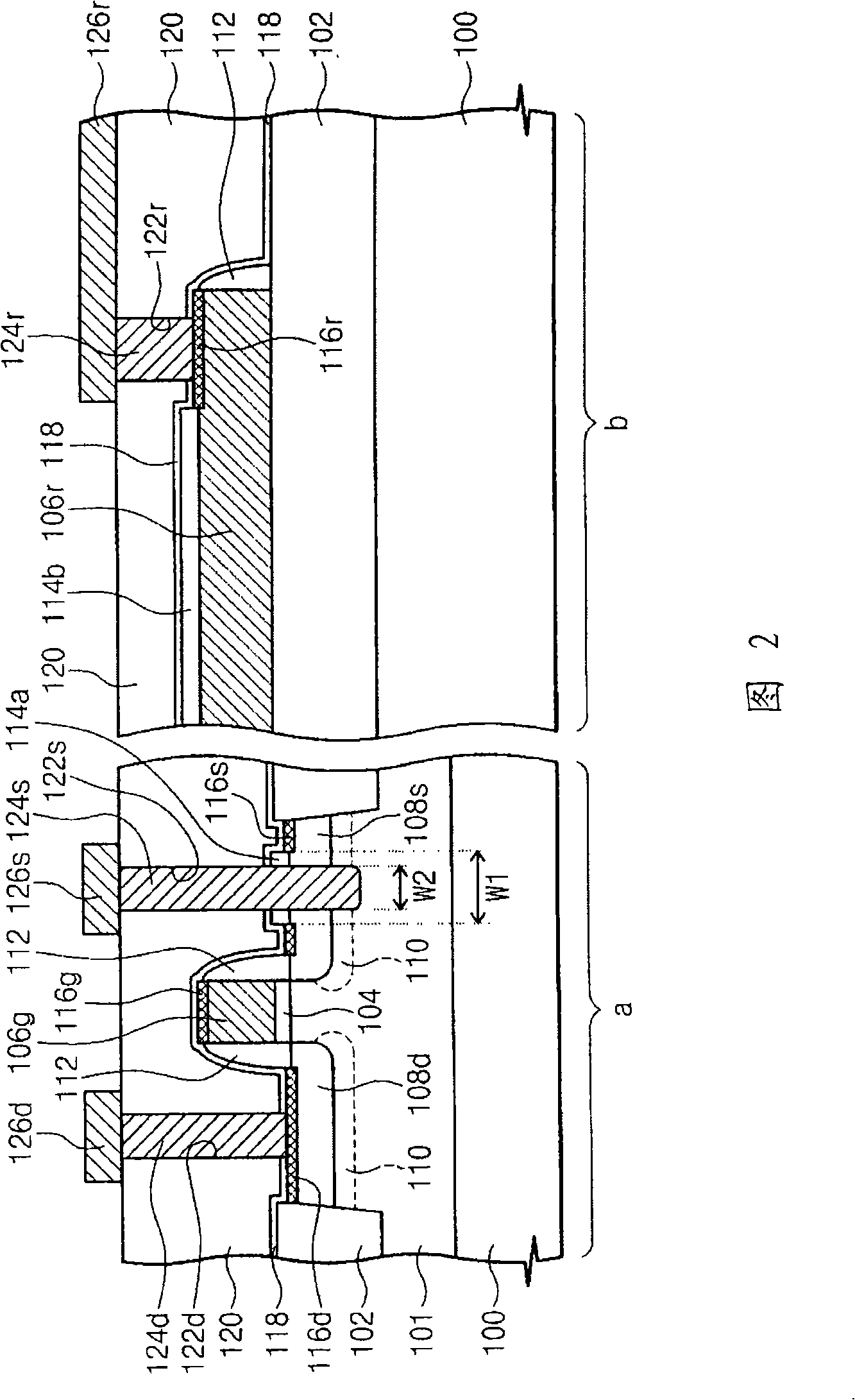
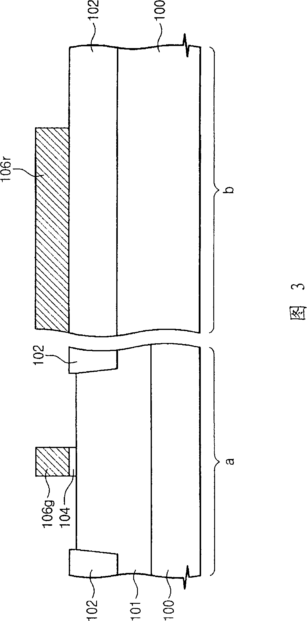
[0030] The present invention will now be described more fully hereinafter with reference to the accompanying drawings in which embodiments of the invention are shown. However, this invention may be embodied in many different forms and should not be construed as limited to the embodiments set forth herein. Rather, these embodiments are provided so that this disclosure will be thorough and complete, and will fully convey the scope of the invention to those skilled in the art. In the drawings, the thicknesses of layers and regions are exaggerated for clarity. Like reference numerals designate like elements throughout.
[0031] It will be understood that when an element or layer is referred to as being "on," "connected to," and / or "coupled to" another element or layer, it can be directly on, connected to, or coupled to the other element or layer. another element or layer, or intervening elements or layers may be present. In contrast, when an element is referred to as being "dir...
PUM
 Abstract
Description
Claims
Application Information
 - R&D
- Intellectual Property
- Life Sciences
- Materials
- Tech Scout
- Unparalleled Data Quality
- Higher Quality Content
- 60% Fewer Hallucinations
Browse by: Latest US Patents, China's latest patents, Technical Efficacy Thesaurus, Application Domain, Technology Topic, Popular Technical Reports.
© 2025 PatSnap. All rights reserved.Legal|Privacy policy|Modern Slavery Act Transparency Statement|Sitemap|About US| Contact US: help@patsnap.com