Apparatus and method for press welding printed circuit to flat display panel

A printed circuit and equipment technology, applied in the direction of circuits, electrical solid devices, instruments, etc., can solve the problems of increased processing time, etc., and achieve the effects of easy bonding process, avoiding damage and cracks, and high-speed bonding process

Inactive Publication Date: 2010-06-30
SFA ENG CORP
View PDF3 Cites 1 Cited by
  • Summary
  • Abstract
  • Description
  • Claims
  • Application Information

AI Technical Summary

Problems solved by technology

However, the problem of an unavoidable increase in processing time is not only due to the fact that the product manufacturer does not want to purchase an expensive and technically complex construction of measuring equipment, but also because of the increased time between the calibration platform's support surface and the auxiliary tool's support surface

Method used


Image

  • Apparatus and method for press welding printed circuit to flat display panel
  • Apparatus and method for press welding printed circuit to flat display panel
  • Apparatus and method for press welding printed circuit to flat display panel

Examples


Embodiment Construction

[0055] The present invention is used to illustrate the drawings attached to the preferred embodiments, so that the examiners can better understand the present invention, its advantages, and achieve the purpose of the present invention. In the following description of the present invention, preferred embodiments of the present invention will be described in detail with reference to the accompanying drawings. Wherein, the same element numbers represent the same elements.

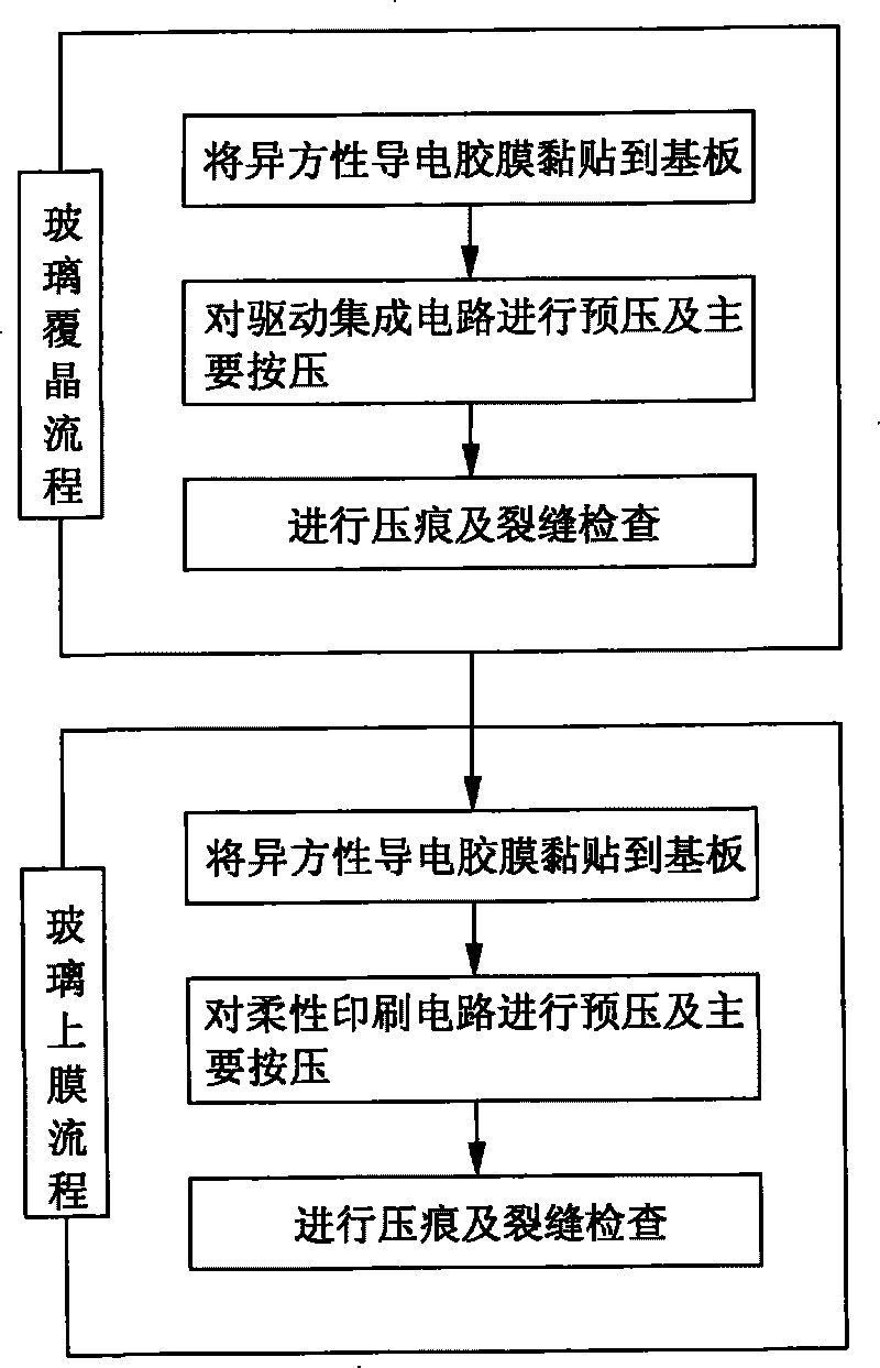
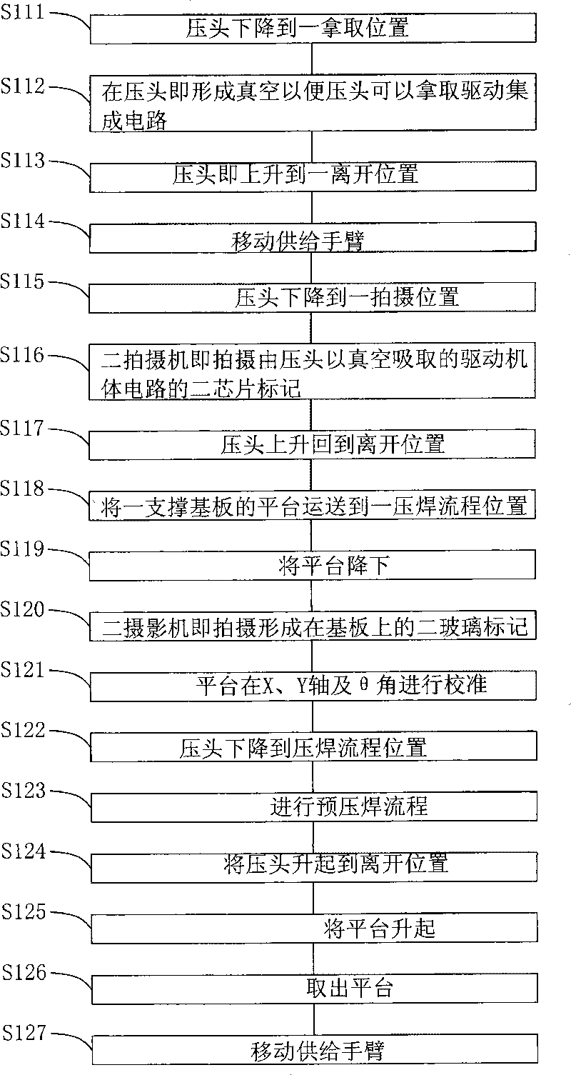
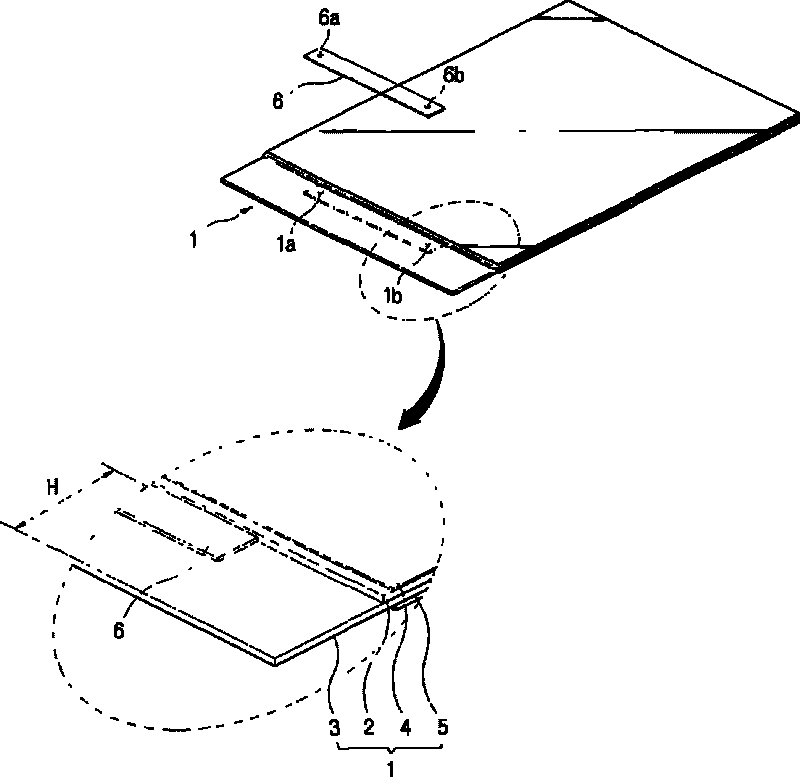
[0056]According to an embodiment of the present invention, an apparatus and method for bonding a printed circuit can be used to bond (pre-bond) a printed circuit to a substrate of a flat panel display (FPD), such as a flexible Printed circuit (FPC), tape and reel chip carrier package (TCP), general batch flexible circuit board (CBF) and driver IC (driver IC), and flat panel display is such as plasma display panel (PDP), liquid crystal display (LCD) and Organic Light Emitting Diodes (OLED). For the convenienc...


PUM

PropertyMeasurementUnit
thicknessaaaaaaaaaa
thicknessaaaaaaaaaa

Abstract

A device for pressure-welding a printing circuit comprising a platform with a supporting surface; the supporting surface is a supporting substrate moving and picking up the substrate to a pressure-welding procedure position; the printing circuit is a pressure-welding substrate; a pressing head provided on the pressure-welding procedure position which can be raised absorbing the printing circuit and being pressure-welded to the substrate opposite to the printing circuit absorbed by the substrate; a device for obtaining the checking video information; at least a chip mark forming on the printing circuit for simultaneous shooting on at least one glass mark on the substrate to obtain the checking video information; thereby, the printing circuit is pressure-welded to the substrate by a simple and convenient method, and processing time of the pressure-welding procedure is shortened to achieve the high-speed pressure-welding procedure.

Description

technical field [0001] The present invention relates to a device and method for obtaining calibration image information and for bonding a printed circuit to a panel of a flat panel display, in particular to a simple and convenient method that simultaneously shortens the length of a bonding process. The processing time of the process is to realize the equipment and method for obtaining and calibrating the image information device of the high-speed pressure welding process and pressure-welding the printed circuit on the panel of the flat panel display. Background technique [0002] Generally speaking, flat panel displays (FPD) such as plasma display panels (plasma display panel, PDP), liquid crystal displays (liquid crystal display, LCD) and organic light emitting diodes (organic light emitting diode, OLED), etc., It is gradually made thinner and lighter. Thus, different printed circuits are directly connected to the flat panel display and manufactured into one integrated pro...

Claims


Application Information

Patent Timeline
Patent Type & Authority Patents(China)
IPC IPC(8): G02F1/1333H05K13/04H05K13/08
CPCG02F1/1303H01L24/75H01L24/85H05K13/04
Inventor 陈明出
Owner SFA ENG CORP
Why Eureka
Try Eureka