Solid-state imaging device and camera
A solid-state imaging device and pixel technology, which is used in image communication, TV, color TV components, etc.
- Summary
- Abstract
- Description
- Claims
- Application Information
AI Technical Summary
Problems solved by technology
Method used
Image

Examples
no. 1 example
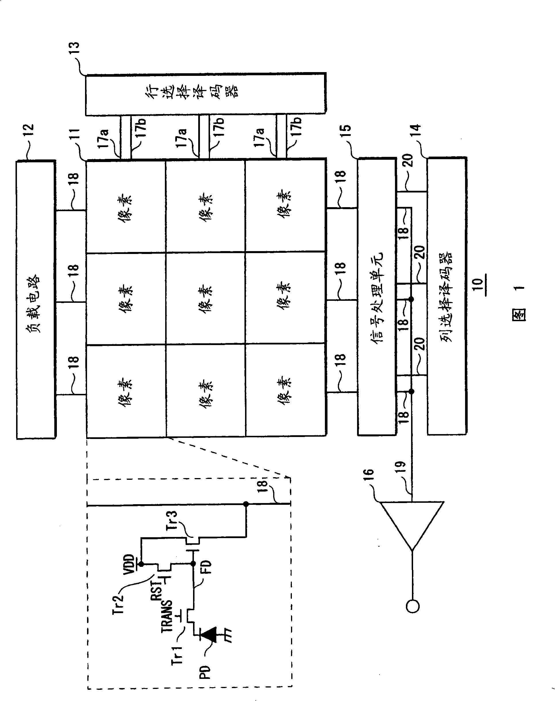
[0059] FIG. 1 shows a general configuration of a solid-state imaging device related to a first embodiment of the present invention.
[0060] The solid-state imaging device 10 includes a pixel array 11 , a load circuit 12 , a row selection decoder 13 , a column selection decoder 14 , a signal processing unit 15 and an output amplifier 16 .
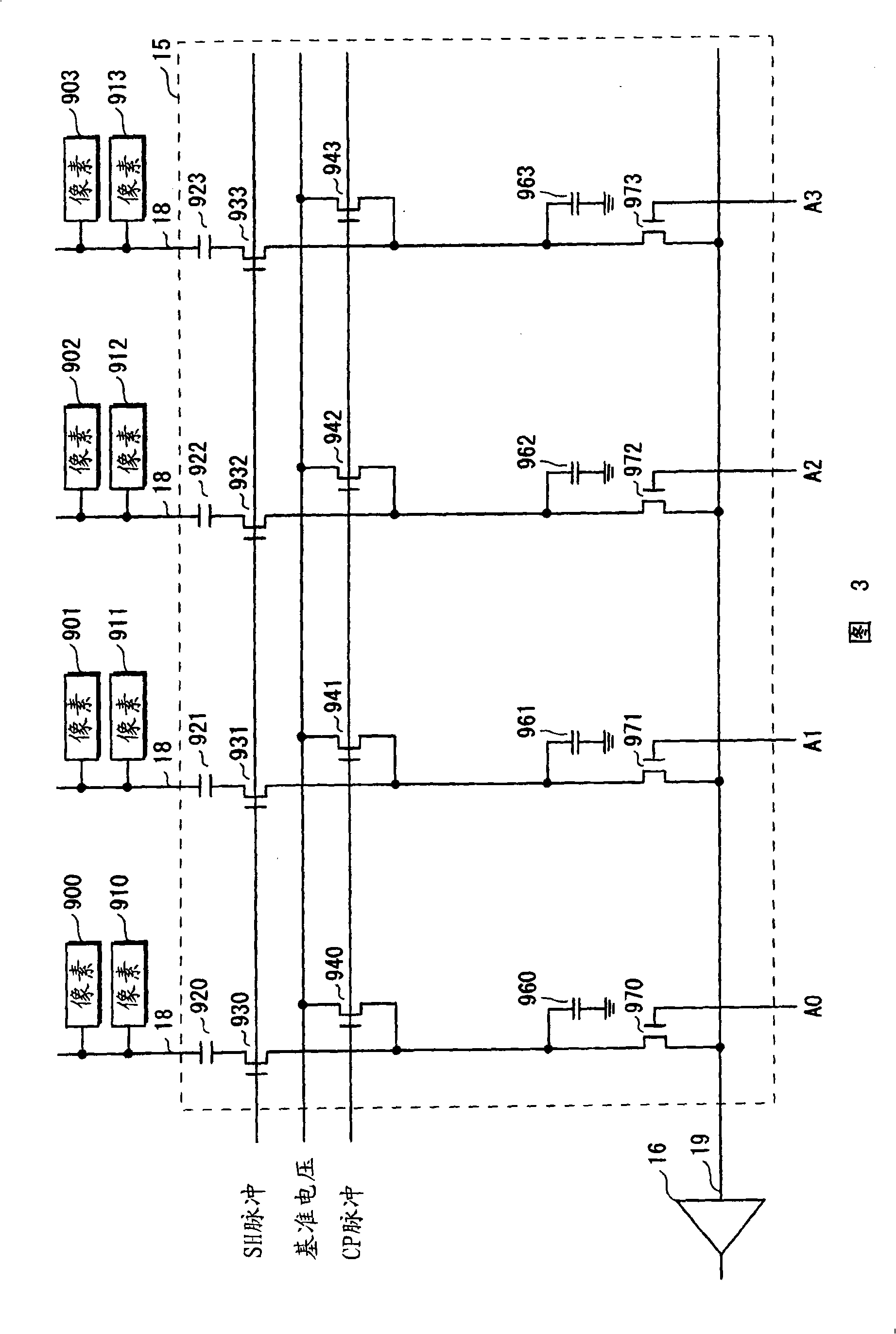
[0061] The pixel array 11 includes a plurality of pixels arranged two-dimensionally. Each pixel includes a photodiode PD, a floating diffusion region FD, and transistors Tr1, Tr2, and Tr3. The gates of the transistors Tr1 and Tr2 are connected to the row signal lines 17a and 17b, respectively. The gate of the transistor Tr3 is connected to the floating diffusion FD, and the source of the transistor Tr3 is connected to the column signal line 18 .
[0062] By receiving various driving pulses from the external timing control unit, the load circuit 12, the row selection decoder 13, the column selection decoder 14, the signal processing unit 1...
no. 2 example
[0085] In the second embodiment, the column-sequential readout of pixel signals is suspended by a method different from that described in the first embodiment. Other features are the same as those of the first embodiment, so descriptions thereof are omitted.
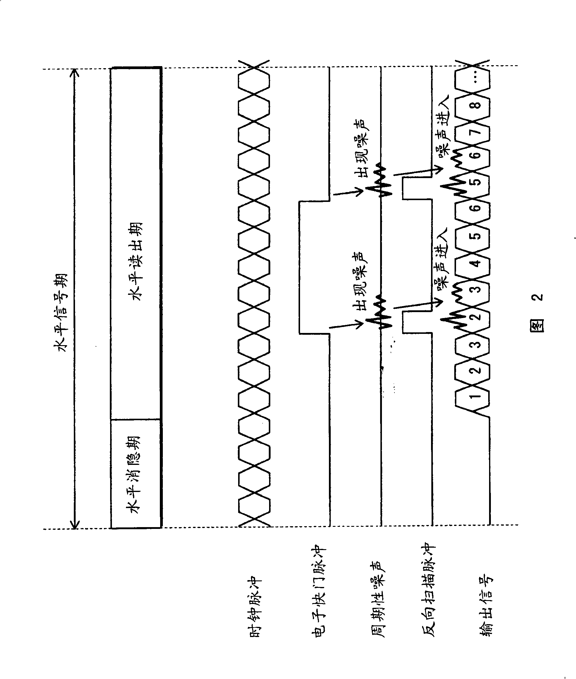
[0086] FIG. 10 shows a readout standby operation for suspending column-sequential readout of pixel signals related to the second embodiment of the present invention.
[0087] In a second embodiment, the column select decoder 14 includes a shift register capable of (i) shifting in the forward direction corresponding to the order of the pixel array columns, and (ii) pausing on receipt of a clock pulse shift operation. The shift register shifts in the forward direction when the level of the cyclic scan pulse is low, and the shift operation is suspended when the level of the cyclic scan pulse is high. The level of the cyclic scanning pulse is designed to be: (i) low level during the horizontal readout period except the rea...
no. 3 example
[0096] The third embodiment differs from the first embodiment in that the output of pixel signals to the outside is restricted in the readout standby period. Other features are the same as those of the first embodiment, so descriptions thereof are omitted.
[0097] FIG. 13 shows a readout standby operation for suspending column-sequential readout of pixel signals related to the third embodiment of the present invention.
[0098] In the third embodiment, the pixel signal is output to the outside when the level of the output limit pulse is low, and the pixel signal is not output to the outside when the level of the output limit pulse is high. The level of the output limit pulse is designed to be low level during the horizontal readout period other than the readout standby period, and to be high level during the readout standby period. By designing the output limiting pulse in the above manner, it is possible to limit the output of unnecessary pixel signals during the readout st...
PUM
 Abstract
Description
Claims
Application Information
 - R&D
- Intellectual Property
- Life Sciences
- Materials
- Tech Scout
- Unparalleled Data Quality
- Higher Quality Content
- 60% Fewer Hallucinations
Browse by: Latest US Patents, China's latest patents, Technical Efficacy Thesaurus, Application Domain, Technology Topic, Popular Technical Reports.
© 2025 PatSnap. All rights reserved.Legal|Privacy policy|Modern Slavery Act Transparency Statement|Sitemap|About US| Contact US: help@patsnap.com