
Adiabatic waveguide transitions

A waveguide and optical waveguide technology, applied in the coupling of optical waveguides, optical guides, instruments, etc., can solve the problems of effective manufacturing difficulties, channel waveguide discontinuity, etc., and achieve the effect of low insertion loss

Inactive Publication Date: 2008-11-26
JDS UNIPHASE CORP
View PDF3 Cites 18 Cited by
  • Summary
  • Abstract
  • Description
  • Claims
  • Application Information

AI Technical Summary

Problems solved by technology

[0004] [04] One problem with the transition between the slab and the channel waveguide output array is that the channel waveguides become discontinuous through the transition
However, the small features of these protrusions and segments make it more difficult to efficiently manufacture

Method used


Image

  • Adiabatic waveguide transitions
  • Adiabatic waveguide transitions
  • Adiabatic waveguide transitions

Examples


Embodiment Construction

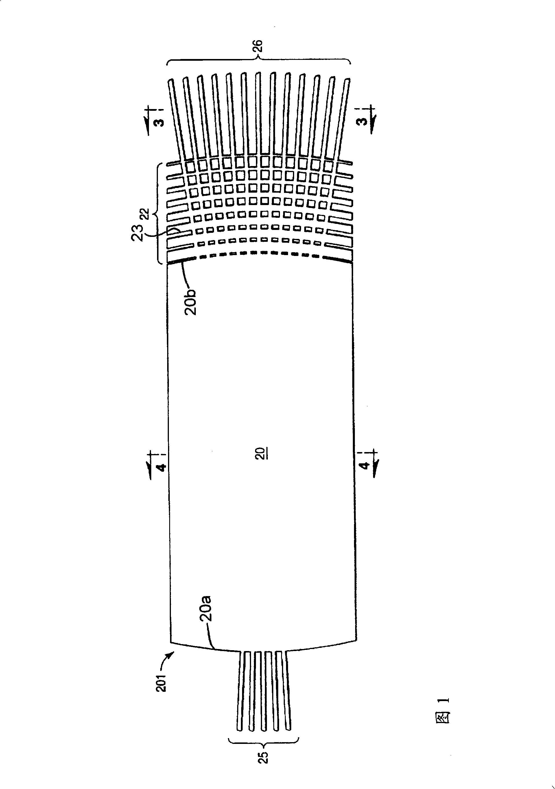
[0047] [32] Referring to FIG. 1, there is shown a prior art star coupler 201 disclosed in US 5,745,618 having a transition region 22 comprising a plurality of silicon material vias 23, typically parallel to each other and transverse to the output waveguide 26 to greatly reduce insertion loss. A star coupler splits the optical power entering any one of its output ports. The star coupler 201 comprises a free space region containing an optical slab waveguide 20 with two curved, preferably circular, boundaries 20a, 20b. Power transmission between the input waveguide array 25 and the output waveguide array 26 is achieved by radiation from the flat panel 20 . These arrays of waveguides 25, 26 are directed radially towards the virtual focus and are configured to set their respective focal lengths at a predetermined distance from the panel 20 such that phase errors due to mutual coupling between adjacent waveguides are minimized. . Each waveguide array is coupled to plate 20 along ...


PUM


Abstract

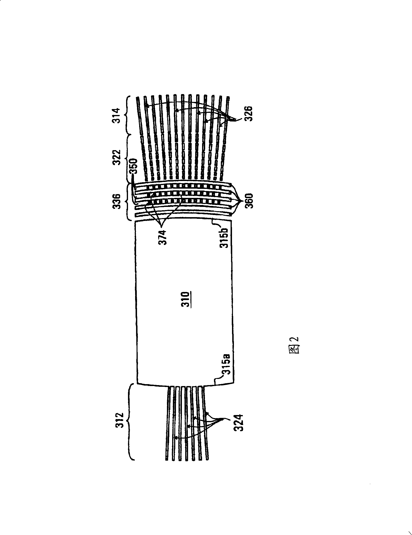
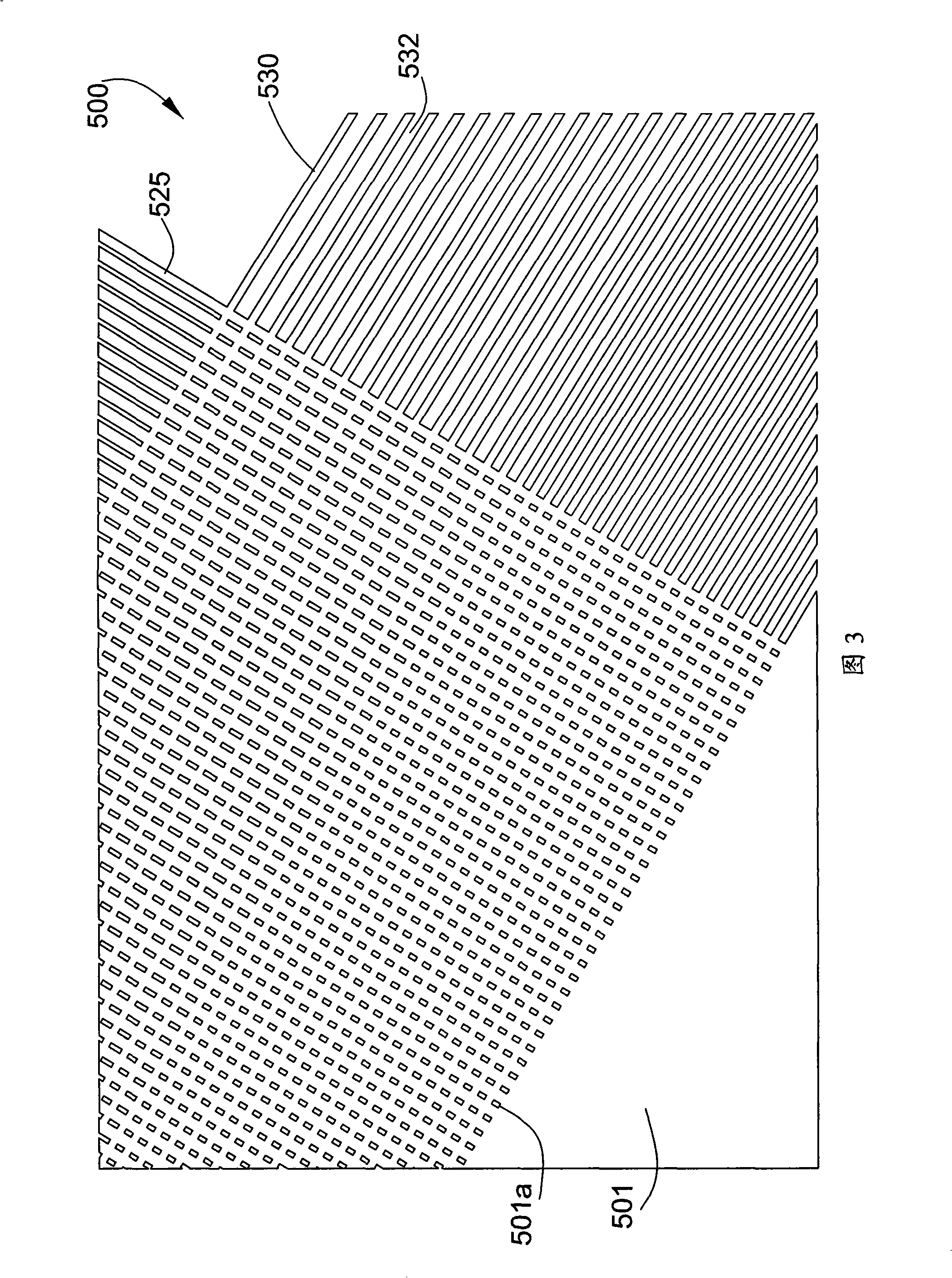
The invention relates to waveguiding structures in planar lightwave circuit devices that include a transition region between a slab waveguide and channel waveguides to reduce optical coupling loss. In particular star couplers and arrayed waveguide gratings incorporating the transition region of the present invention demonstrate reduced insertion loss. By creating a transition region composed of transverse rows intersecting the output waveguide array, where the rows have equal dimensions and the effective refractive index is controlled by increasing the spacing width gradually from row to row, an adiabatic transition is created from slab waveguide to channel waveguide array. This structure provides low insertion loss within practical manufacturing tolerances. In addition, the present invention has found that by incorporating the transition region of the present invention into an AWG, the reduced insertion loss can be controlled as uniform insertion loss across the channels.

Description

technical field [0001] [01] The present invention relates to an optical device formed in a planar lightwave circuit that includes a transition region between a slab waveguide and a channel waveguide to reduce optical losses. In particular, the present invention encompasses star couplers and arrayed waveguide grating (AWG) devices that include transition regions that reduce losses. Background technique [0002] [02] Currently, optical communication networks rely on planar lightwave line (PLC) devices such as star couplers, branch power splitters, and arrayed waveguide gratings (AWGs) and variable optical attenuators (VOAs) to simultaneously control the entire network Many wavelength multiplexed optical signals. [0003] [03] A PLC comprises an optical waveguide that is deposited and patterned on a substrate. In one common technique, a doped silica core and cladding are deposited and patterned on a silica or silicon substrate. Other substrate and waveguide technologies can ...

Claims


Application Information

Patent Timeline
Patent Type & Authority Applications(China)
IPC IPC(8): G02B6/125G02B6/34
CPCG02B6/12011G02B6/12014
Inventor 巴特勒米·方达埃德蒙·J.·墨菲罗伯特·J.·布雷纳德
Owner JDS UNIPHASE CORP
Learn More