

Semiconductor device and method of manufacturing the same
A semiconductor and device technology, applied in the field of semiconductor devices, can solve problems such as uneven fuse stress distribution, increased fuse resistance, and changing physical properties.
- Summary
- Abstract
- Description
- Claims
- Application Information
AI Technical Summary
Problems solved by technology
Method used
Image

Examples
no. 1 example
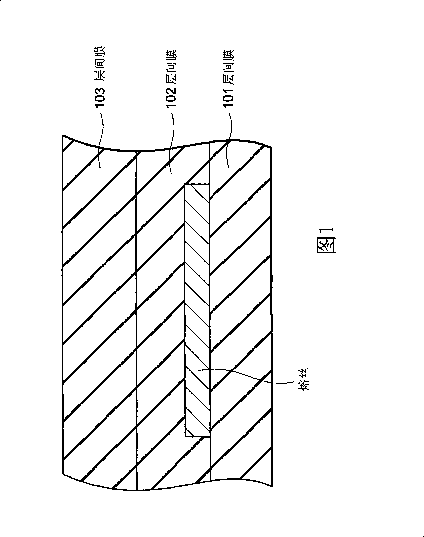
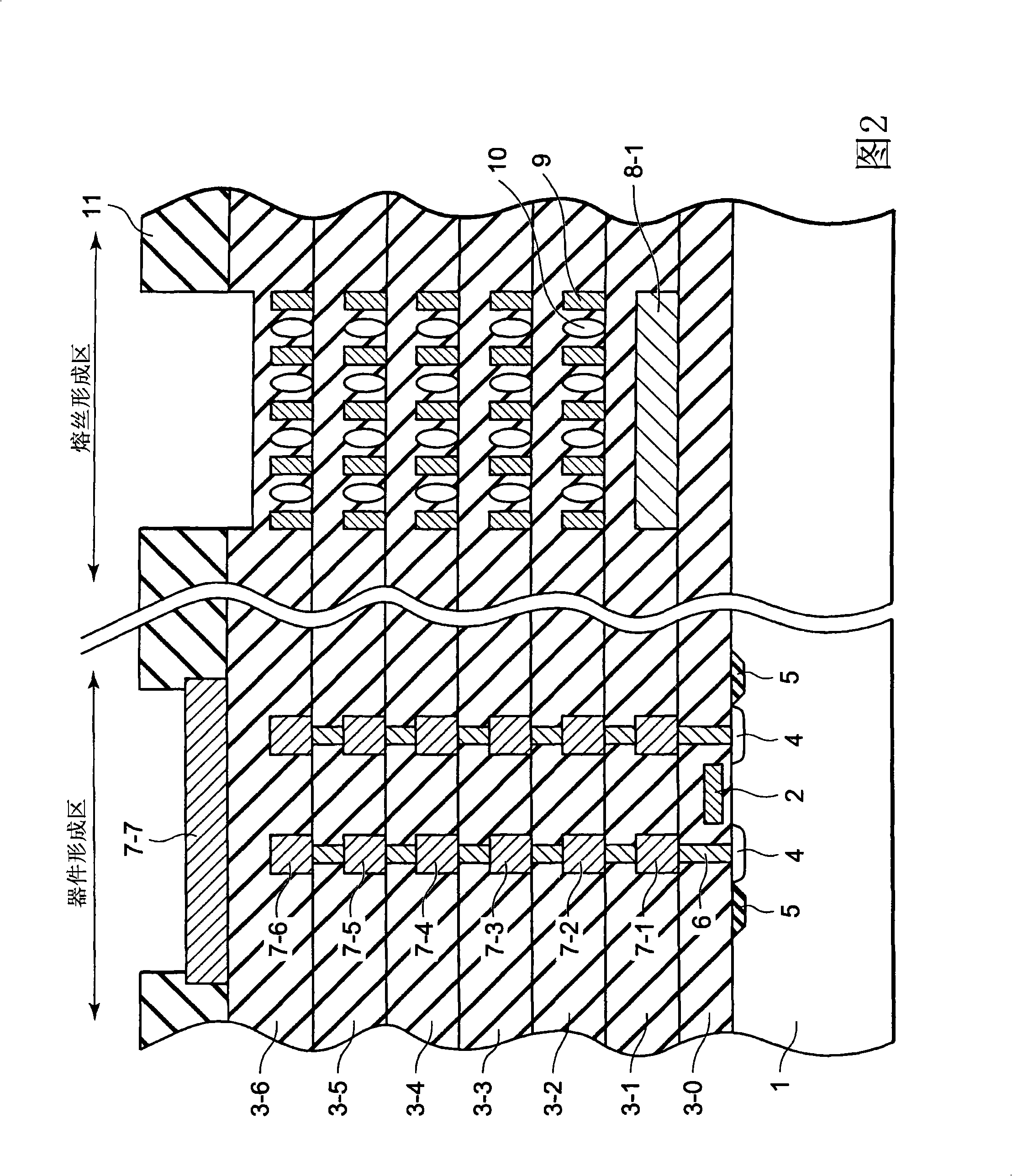
[0027] Hereinafter, embodiments of the present invention will be described with reference to the accompanying drawings. 2 is a schematic cross-sectional view showing the structure before the fuse is blown in the semiconductor device of the present embodiment. The semiconductor device includes a substrate 1 (for example, a silicon substrate), a plurality of insulating films 3-0 to 3-6 (for example, a silicon dioxide film) formed on the substrate 1, and an interlayer insulating film covering the uppermost layer. Passivation film 11 (for example, silicon oxide film) of film 3-6. In addition, the semiconductor device is provided with a device formation region where semiconductor transistors and the like are formed, and a fuse formation region where fuses are formed.
[0028] In the device formation region, isolation regions 5 and source / drain regions 4 are formed on the surface of substrate 1 . A first insulating film 3 - 0 is also formed on the surface of the substrate 1 . Gat...
no. 2 example
[0054] Next, a second embodiment will be explained. FIG. 6 is a schematic cross-sectional view showing the structure of the semiconductor device of the present embodiment. In the first embodiment, the case has been described in which the fuse 8-1 and the interconnection 7-1 in the device formation region are formed of the same material and in the same step. However, in the present embodiment, the fuse 8-2 is formed in the same step as the gate electrode 2 of the semiconductor transistor. The rest of the structure is the same as in the first embodiment, and therefore, will not be described in detail.
[0055] As shown in FIG. 6, the gate electrode 2 is formed in the insulating film 3-0 in the device formation region. Gate electrode 2 is formed of polysilicon. In addition, the fuse 8-2 is buried in the insulating film 3-0 (first insulating film) in the fuse formation region. Like the gate electrode 2, the fuse 8-2 is formed of polysilicon. Gate electrode 2 and fuse 8-2 are ...
no. 3 example
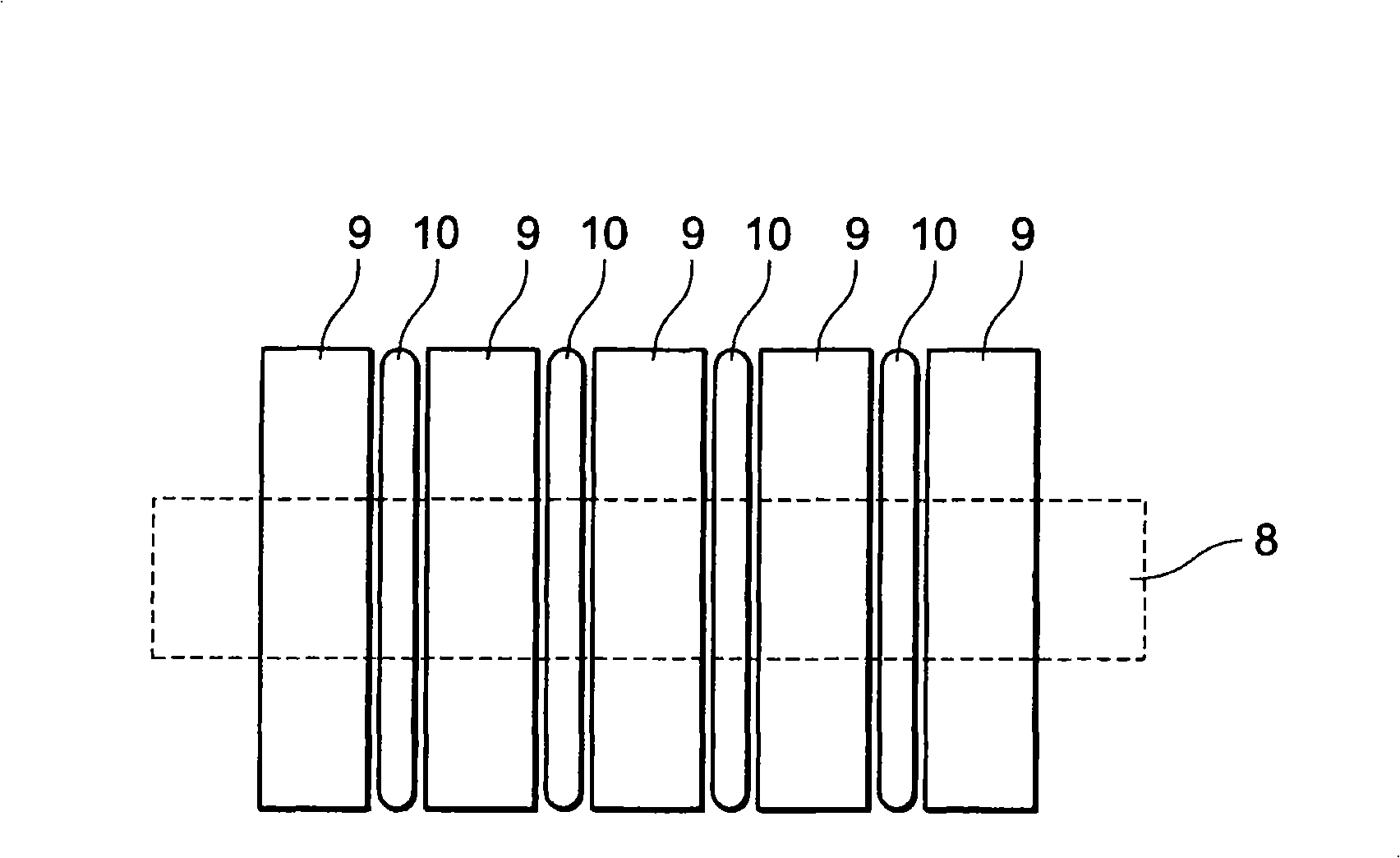
[0059] Subsequently, a third embodiment will be explained. FIG. 7 is a schematic cross-sectional view showing the structure of the semiconductor device of the present embodiment. In the first embodiment, the case has been described in which the fuse 8-1 and the interconnection 7-1 in the device formation region are formed of the same material and in the same step. However, in the present embodiment, the fuse 8-3 and the interconnection 7-4 in the device formation region are formed of the same material and in the same step. That is, the fuse 8-3 is provided in the insulating film 3-4 (on the insulating film 3-3).
[0060] In this embodiment, hole forming patterns 9 and holes 10 are provided on insulating films 3-4 and 3-5. That is, holes 10 are provided in the insulating films 3-5 and 3-6 (second insulating films). Neither the hole forming pattern 9 nor the hole 10 is formed in a layer not lower than the insulating film 3-4 (first insulating film).
[0061] The rest of the ...
PUM
 Abstract
Description
Claims
Application Information