Method for verifying whether detection result of detection device is correct or not

A technology for testing equipment and testing results, applied in static memory, instruments, etc., can solve the problems of low chip power supply voltage, large influence range, and inability to see the underlying structure, etc., and achieve the effect of precise positioning

Inactive Publication Date: 2009-01-21
SEMICON MFG INT (SHANGHAI) CORP
View PDF0 Cites 2 Cited by
  • Summary
  • Abstract
  • Description
  • Claims
  • Application Information

AI Technical Summary

Problems solved by technology

When there are many metal layers on the chip, the underlying structure cannot be seen, so when dotting, it is impossible to determine the specific location of the dot
If you do it rashly, for static memory, it is easy to connect the power supply voltage line and the ground point of the chip, which may eventually cause the p

Method used


Image

  • Method for verifying whether detection result of detection device is correct or not
  • Method for verifying whether detection result of detection device is correct or not

Examples


Embodiment Construction

[0011] A preferred embodiment of the method for verifying whether the detection result of the detection device of the present invention is correct will be described in further detail below in conjunction with the accompanying drawings.

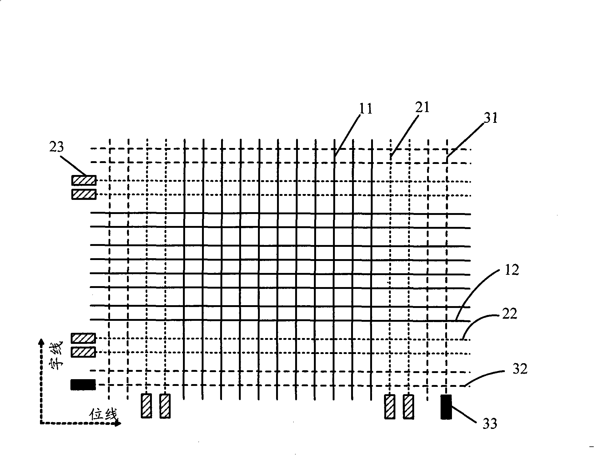
[0012] figure 1 It is a simplified schematic diagram in the form of a chip matrix, where the horizontal bit line is the bit line, the vertical word line is the word line, and the intersection of each bit line and each word line is a memory cell. A chip usually includes a working area and a dummy area (dummy) and a spare area (redundancy) located on the periphery of the working area. The active area includes bit lines 12 and word lines 11 . The dummy area includes the bit line 32 and the word line 31, both of which are located in the outermost layer of the working area of ​​the chip, which protect the working area and do not participate in the actual circuit work. The spare area includes bit lines 22 and word lines 21. The spare area is opera...


PUM


Abstract

The invention discloses a method for verifying whether a detection result of a detecting device is right, which relates to the detecting technology of semiconductors. The method comprises a clip which is equipped with a work area and a nominal area, the clip comprises a plurality of bit lines and word lines, the nominal area does not participate in a circuit work of the work area, and the bit lines or the word lines of the nominal area are connected with fuse wires and are connected with preinstall bit lines or word line circuits of the work area. The preinstall bit lines or the word lines of the work area fail through that the fuse wires are interrupted, the bit lines or the word lines of the nominal area which are connected with the fuse wires replace the preinstall bit lines or preinstall word lines of the work area, thereby obtaining an invalid practical physical address. The clip is detected by the detecting device, thereby outputting a detected physical address, and whether the detecting device is natural can be detected through comparing the practical physical address and the detected physical address. Compared with the prior art, the fuse wires are bigger and are conveniently interrupted by focusing ions or lasers. The design of a fuse wire circuit is added in the nominal area, and the whole area of the clip does not need to be increased.

Description

technical field [0001] The invention relates to a semiconductor detection process, in particular to a method for verifying whether the detection result of a detection device is correct. Background technique [0002] For problematic memory products reported by customers, it is often necessary to conduct physical failure analysis to find out the problem. The process of physical failure analysis is to detect the faulty storage unit by testing equipment, and output the physical address of the storage unit on the memory chip; then perform various analyzes according to the output physical address, and finally find out the problem. But sometimes, due to the error of the program design of the detection device itself, the output physical address is wrong. If you analyze it based on the wrong physical address, you will get nothing, and you will not be able to find the real problem. Therefore, before analyzing the cause of failure, it is often necessary to verify whether the detectio...

Claims


Application Information

Patent Timeline
IPC IPC(8): G11C29/44
Inventor 张启华廖炳隆陈强王君丽
Owner SEMICON MFG INT (SHANGHAI) CORP
Why Eureka
Try Eureka